48 www.xilinx.com AC701 Evaluation Board
UG952 (v1.3) April 7, 2015
Chapter 1: AC701 Evaluation Board Features
Table 1-21 lists the connections between the FPGA and the LCD header. If the LCD is not
installed, the J23 pins listed in Table 1-21 can be used for GPIO.
For the Displaytech S162DBABC LCD data sheet, see [Ref 23].
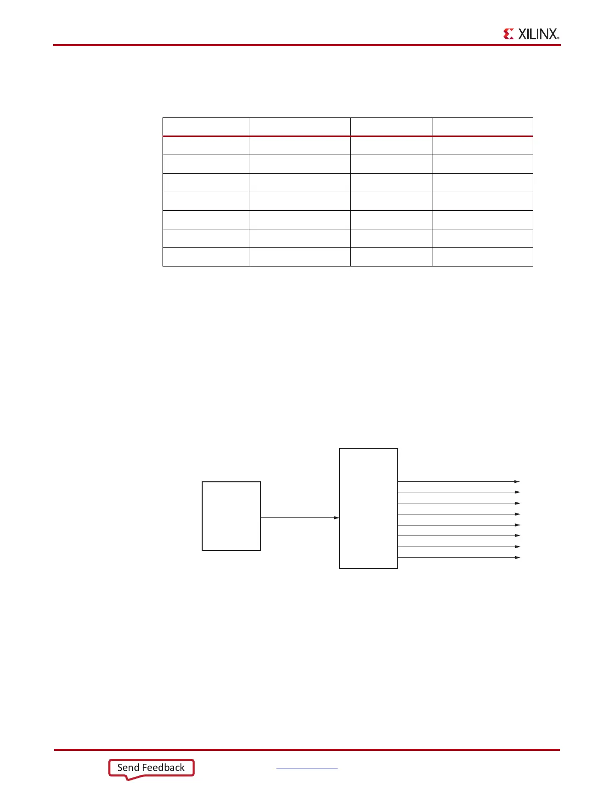
I2C Bus Switch
[Figure 1-2, callout 19]
The AC701 board implements a single I2C port on FPGA Bank 14 (IIC_SDA_MAIN, FPGA
pin K25 and IIC_SCL_MAIN, FPGA pin N18), which is routed through a Texas
Instruments PCA9548 1-to-8 channel I2C switch (U52). The I2C switch can operate at
speeds up to 400
kHz. The U52 bus switch at I2C address 0x74/0b01110100 must be
addressed and configured to select the desired target downstream device.
The AC701 board I2C bus topology is shown in Figure 1-29.
User applications that communicate with devices on one of the downstream I2C buses
must first set up a path to the desired bus through the U52 bus switch at I2C address
0x74/0b01110100.
Table 1-21: FPGA to LCD Header Connections
FPGA Pin (U1) Schematic Net Name I/O Standard LCD Header Pin (J23)
L25 LCD_DB4_LS LVCMOS33 4
M24 LCD_DB5_LS LVCMOS33 3
M25 LCD_DB6_LS LVCMOS33 2
L22 LCD_DB7_LS LVCMOS33 1
L24 LCD_RW_LS LVCMOS33 10
L23 LCD_RS_LS LVCMOS33 11
L20 LCD_E_LS LVCMOS33 9
X-Ref Target - Figure 1-29
Figure 1-29: I2C Bus Topology
PCA9548
1
2
C 1-to-8
Bus Switch
CH7 - SI5324_SDA/SCL
U52
IIC_SDA/SCL_MAIN
CH6 - IIC_SDA/SCL_DDR3
CH5 - IIC_SDA/SCL_HDMI
CH4 - SFP_IIC_SDA/SCL
CH3 - EEPROM_IIC_SDA/SCL
CH2 - (NOT USED)
CH1 - FMC_HPC_IIC_SDA/SCL
CH0 - USER_CLK_SDL/SCL
FPGA
Bank 14
(3.3V)
0x74
U1
UG952_C1_27_100312

 Loading...


