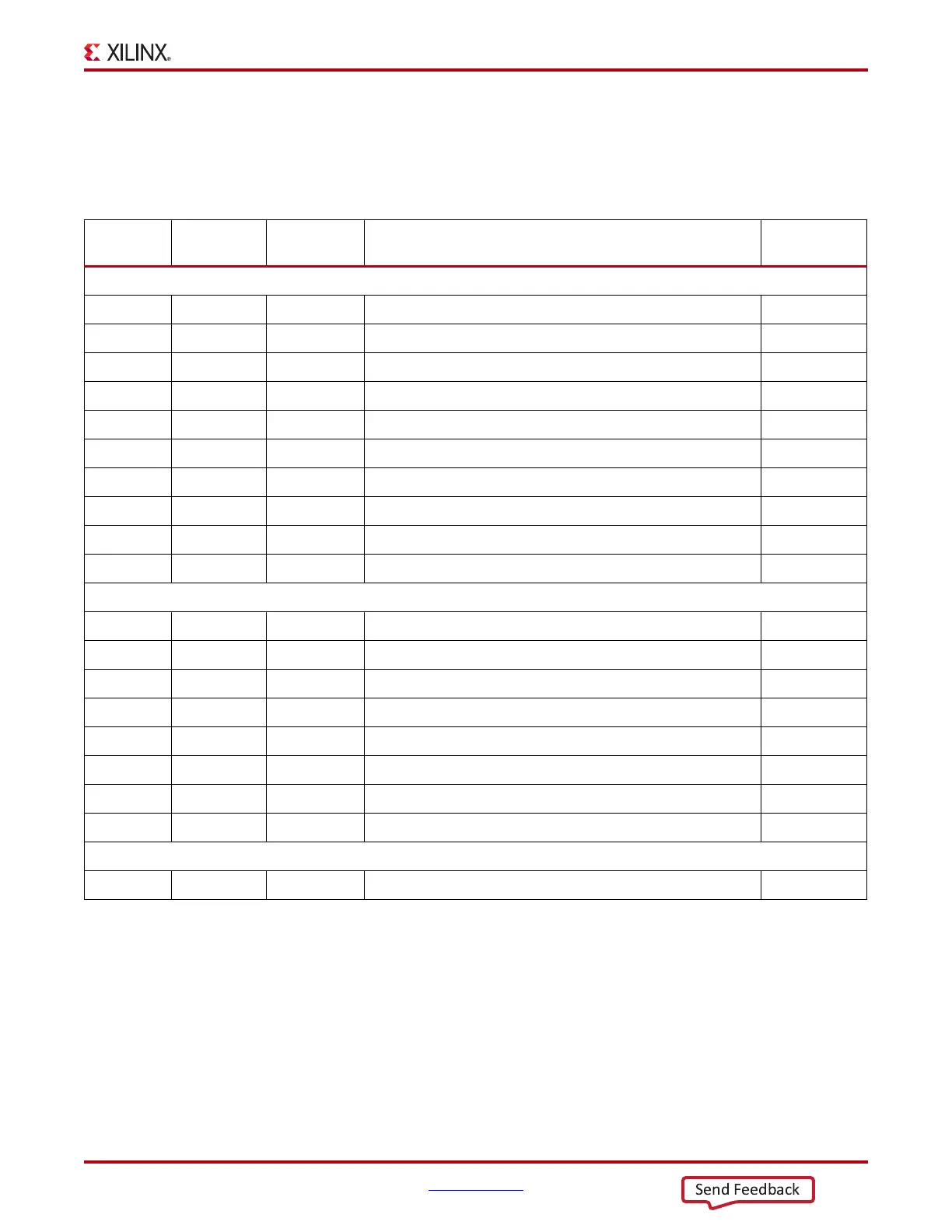
Default Jumper Settings
AC701 Evaluation Board www.xilinx.com 81
UG952 (v1.3) April 7, 2015
Default Jumper Settings
The AC701 board default jumper configurations are listed in Table A-3. The AC701 board
jumper header locations are shown in Figure A-3.
Table A-3: AC701 Default Jumper Settings
Callout
Header Ref
Des
Jumper
Position
Description
Schematic
0381502 Page
2-pin
1 J3 None SPI SELECT = onboard SPI flash memory device 4
2 J5 1-2 EPHY U12.2 CONFIG2 = LOW 15
3 J6 1-2 P3 SFP+ TX enabled 20
4 J8 1-2 VCCO_VADJ (FMC) voltage = ON 45
5 J9 1-2 U35 REF3012 XADC_AGND L3 bypassed 29
6 J10 1-2 U35 REF3012 XADC_AGND = GND 29
7 J11 1-2 XADC V
CCINT
4A range 34
8 J52 None J52.1 INIT_B, J51.2 DONE test header, not a jumper 7
9 J53 1-2 XADC_VCC5V0 = 5V 29
10 J63 None Voltage regulators enabled 38
3-pin
11 J35 1-2 EPHY U12.3 CONFIG3 = HI 15
12 J36 None EPHY U12.2 CONFIG2 option header 15
13 J37 None EPHY U12.3 CONFIG3 option header 15
14 J38 1-2 SFP RX BW = FULL 20
15 J39 1-2 SFP TX BW = FULL 20
16 J42 1-2 XADC_VREFP = REF3012 XADC_VREF 29
17 J43 2-3 XADC_VCC = ADP123 1.85V 29
18 J54 2-3 REF3012 V
IN
= XADC_VCC 29
2x2
19 J12 3-4 PCIE lane width = 4 28

 Loading...


