AC701 Evaluation Board www.xilinx.com 23
UG952 (v1.3) April 7, 2015
Feature Descriptions
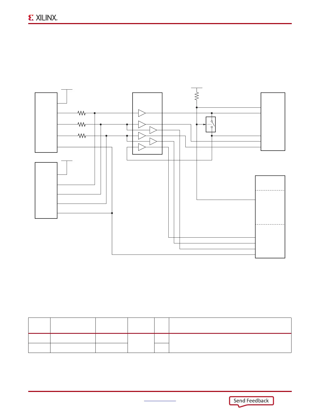
The JTAG connectivity on the AC701 board allows a host computer to download
bitstreams to the FPGA using Xilinx software tools. In addition, the JTAG connector allows
debug tools or a software debugger to access the FPGA. Xilinx software tools can also
indirectly program the Quad SPI flash memory. To accomplish this, Xilinx software
configures the FPGA with a temporary design to access and program the Quad SPI flash
memory device. The JTAG circuit is shown in
Figure 1-9.
Clock Generation
There are three clock sources available for the FPGA logic on the AC701 board (see
Table 1-8).
X-Ref Target - Figure 1-9
Figure 1-9: JTAG Circuit
UG952_c1_09_101512
JTAG_TDI
FMC_TDI_BUF
FPGA_TDO
FPGA_TMS_BUF
FPGA_TCK_BUF
FPGA_TDI_BUF
FMC1_TDO_FPGA_TDI
FMC1_HPC_TMS_BUF
FMC1_HPC_PRSNT_M2C_B
JTAG_TMS
JTAG_TCK
JTAG_TDO
FMC1_HPC_TCK_BUF
FMC1 HPC
Connector
TDI
TDO
J30
TMS
TCK
PRSNT_L
VCC3V3
Artix-7
FPGA
TDI
N16
TDO
U1
TMS
TCK
Digilent
USB-JTAG
Module
TMS
TDI
SN74LV541A
Buffer
U19
R95 15Ω
U26
R96 15Ω
R94 15Ω
TCK
TDO
TMS
TDI
J4
TCK
TDO
JTAG
Header
VCC3V3
VCC3V3
U27
Bank 0
Bank 14
Table 1-8: AC701 Board Clock Sources
FPGA
Pin (U1)
Schematic Net
Name
I/O Standard
Clock
Reference
Pin Description
R3 SYSCLK_P LVDS_25
U51
4 SiT9102 2.5V LVDS 200 MHz Fixed Frequency
Oscillator (SiTime). See
System Clock Source, page 25.
P3 SYSCLK_N LVDS_25 5

 Loading...


