20 www.xilinx.com AC701 Evaluation Board
UG952 (v1.3) April 7, 2015
Chapter 1: AC701 Evaluation Board Features
SPI Flash Memory External Programming Header
In addition to the Quad SPI device FPGA U1 connections shown in Table 1-5, the FPGA U1
SPI flash memory interface is connected to an external programming header J7.
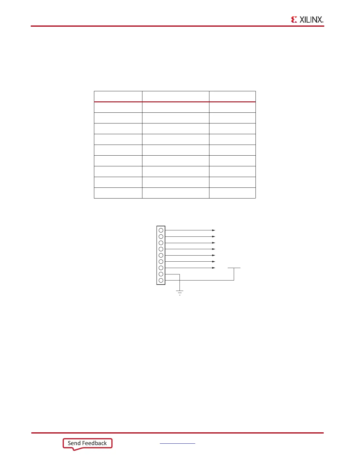
Table 1-6 shows the SPI flash memory J7 connections to FPGA U1.
Figure 1-6 shows the J7 SPI flash memory external programming connector.
Table 1-6: SPI Flash Memory J7 Connections to the FPGA
U1 FPGA Pin Schematic Net Name J7 Pin
AE16 FPGA_PROG_B 1
N14 FLASH_D3 2
P14 FLASH_D2 3
J3.2 QSPI_CS_B 4
R14 FLASH_D0 5
R15 FLASH_D1 6
H13 FPGA_CCLK 7
NA GND 8
NA VCC3V3 9
X-Ref Target - Figure 1-6
Figure 1-6: SPI Flash Memory J7 External Programming Connector
UG952_c1_06_092812
VCC3V3
GND
2
3
4
6
8
7
5
9
FLASH_D3
FLASH_D2
QSPI_CS_B
FLASH_D0
FLASH_D1
FPGA_CCLK
1
FPGA_PROG_B
J7
HDR
1X9

 Loading...


