AC701 Evaluation Board www.xilinx.com 19
UG952 (v1.3) April 7, 2015
Feature Descriptions
Quad SPI Flash Memory
[Figure 1-2, callout 3]
The Quad SPI flash memory U7 provides 256 Mb of nonvolatile storage that can be used
for configuration and data storage.
• Part number: N25Q256A13ESF40G (Micron)
• Supply voltage: 3.3V
• Datapath width: 4 bits
• Data rate: various depending on Single/Dual/Quad mode and CCLK rate
Four data lines and the FPGA CCLK pin are wired to the Quad SPI flash memory. The
connections between the SPI flash memory and the FPGA are listed in
Table 1-5.
The configuration section of the 7 Series FPGAs Configuration User Guide (UG470) [Ref 5]
provides details on using the Quad SPI flash memory. Figure 1-5 shows the connections of
the Quad SPI flash memory on the AC701 board. For more details, see the Micron
N25Q256A13ESF40G data sheet
[Ref 15].
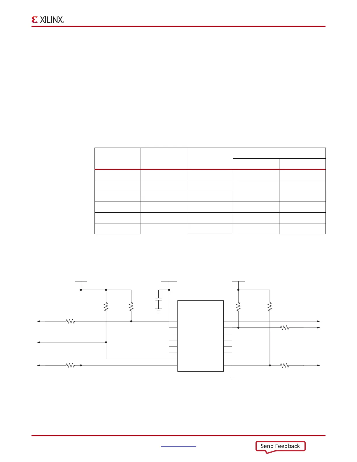
Table 1-5: Quad SPI Flash Memory Connections to the FPGA
FPGA Pin (U1)
Schematic Net
Name
I/O Standard
U7 Quad SPI Flash Memory
Pin Number Pin Name
R14 FLASH_D0 LVCMOS33 15 DQ0
R15 FLASH_D1 LVCMOS33 8 DQ1
P14 FLASH_D2 LVCMOS33 9 DQ2
N14 FLASH_D3 LVCMOS33 1 DQ3
H13 FPGA_CCLK LVCMOS33 16 C
P18 QSPI_IC_CS_B LVCMOS33 7 S_B
X-Ref Target - Figure 1-5
Figure 1-5: 256 Mb Quad SPI Flash Memory
UG952_c1_05_060514
VCC3V3
N25Q256
256 Mb Serial
Flash Memory
GND
1
2
3
5
7
6
U7
4
8
VCC3V3
C18
0.1μF 25V
X5R
FLASH_D2
DQ1
16
15
14
12
10
11
13
9
SB
NC3
NC2
NC1
NC0
VCC
HOLD_B/DQ3
WB/VPP/DQ2
VSS
NC4
NC5
NC6
NC7
DQ0
C
R17
DNP
R18
4.7kΩ 5%
R431
15Ω 1%
R432
15Ω 1%
FLASH_D0
FPGA_CCLK
FLASH_D2_R
FLASH_D0_R
GND
VCC3V3
R20
DNP
R19
4.7kΩ 5%
R21
4.7kΩ 5%
R430
15Ω 1%
R429
15Ω 1%
FLASH_D2_R
FLASH_D3_R
FLASH_D3
FLASH_D1
QSPI_IC_CS_B

 Loading...


