AC701 Evaluation Board www.xilinx.com 57
UG952 (v1.3) April 7, 2015
Feature Descriptions
The default mode setting is M[2:0] = 001, which selects Master SPI flash memory at board
power-on.
See 7 Series FPGAs Configuration User Guide (UG470) [Ref 5] for further details on
configuring the 7 series FPGAs.
FPGA Mezzanine Card Interface
[Figure 1-2, callout 29]
The AC701 board supports the VITA 57.1 FPGA mezzanine card (FMC) specification by
providing high pin count (HPC) connector J30. HPC J30 is keyed so that a the mezzanine
card faces away from the AC701 board when connected.
Signaling speed ratings:
• Single-ended: 9 GHz (18 Gb/s)
• Differential optimal vertical: 9 GHz (18 Gb/s)
• Differential optimal horizontal: 16 GHz (32 Gb/s)
• High density vertical: 7 GHz (15 Gb/s)
The Samtec connector system is rated for signaling speeds up to 9 GHz (18 Gb/s) based on
a –3 dB insertion loss point within a two-level signaling environment.
Connector type:
• Samtec SEAF series, 1.27 mm (0.050 in) pitch. Mates with SEAM series connector
For more information about SEAF series connectors, go to the Samtec website [Ref 19].
HPC Connector J30
[Figure 1-2, callout 29]
The 400-pin HPC connector defined by the FMC specification (Figure B-1, page 83)
provides connectivity for up to:
• 160 single-ended or 80 differential user-defined signals
• 10 GTP transceivers
•2 GTP transceiver clocks
•4 differential clocks
• 159 ground and 15 power connections
The connections between the HPC connector at J30 and FPGA U1 (Table 1-26) implements
a subset of this connectivity:
• 58 differential user defined pairs
• 34 LA pairs (LA00-LA33)
• 24 HA pairs (HA00-HA23)
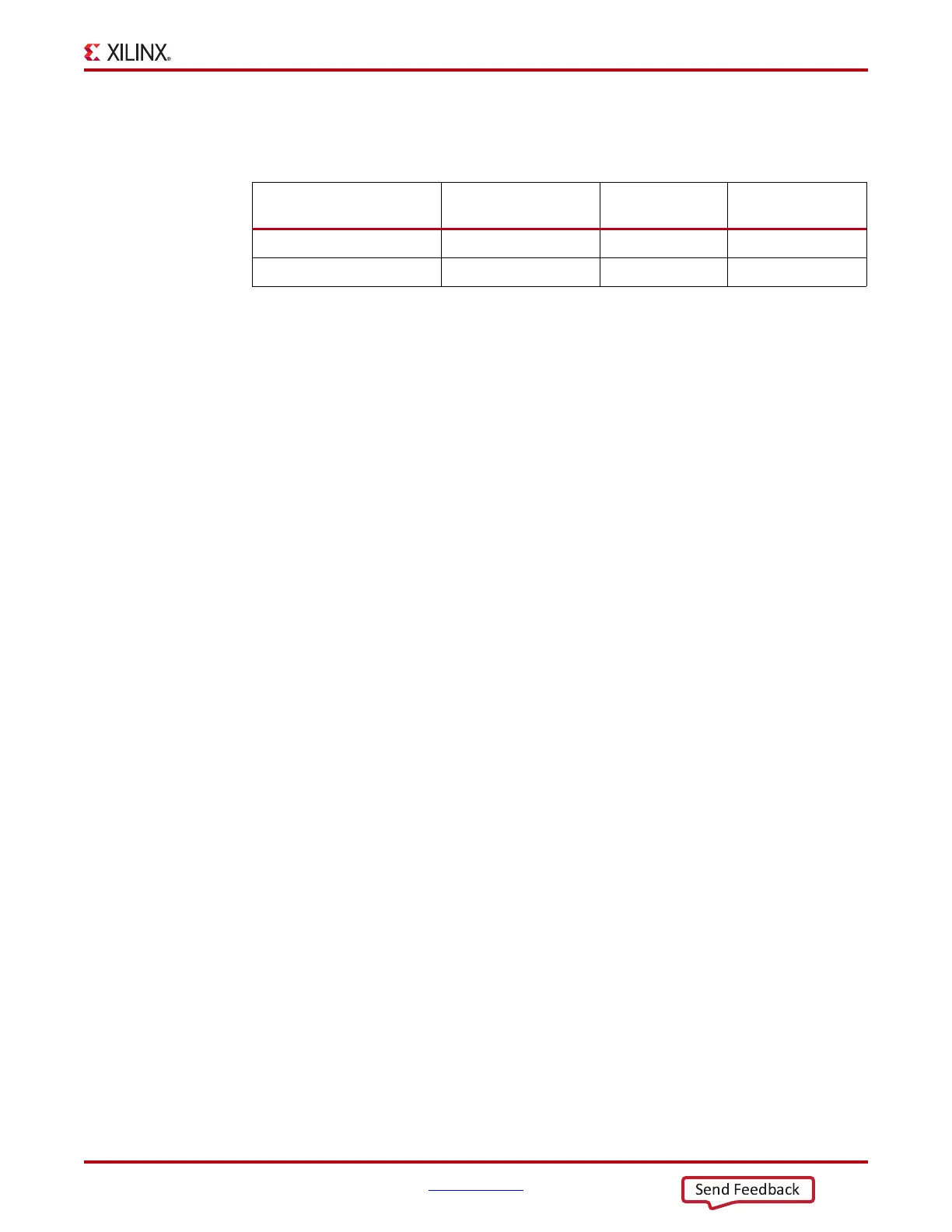
Table 1-25: AC701 Board FPGA Configuration Modes
Configuration Mode
SW13 DIP Switch
Settings (M[2:0])
Bus Width CCLK Direction
Master SPI flash memory 001 x1, x2, x4 Output
JTAG 101 x1 Not Applicable

 Loading...


