56 www.xilinx.com AC701 Evaluation Board
UG952 (v1.3) April 7, 2015
Chapter 1: AC701 Evaluation Board Features
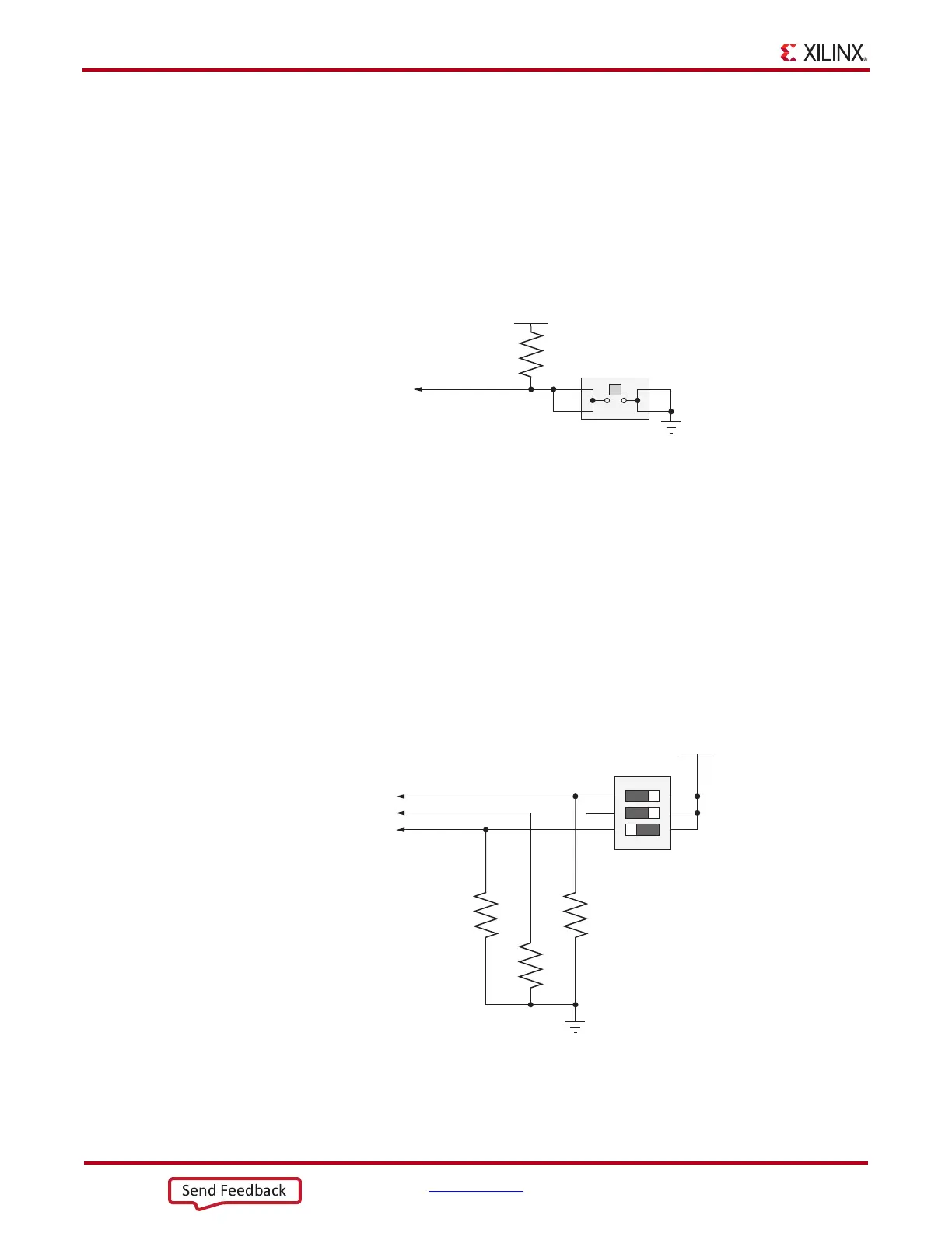
FPGA_PROG_B Pushbutton SW9 (Active-Low)
[Figure 1-2, callout 27]
Switch SW9 grounds the FPGA PROGRAM_B pin when pressed. This action initiates an
FPGA reconfiguration. The FPGA_PROG_B signal is connected to FPGA U1 pin AE16.
See 7 Series FPGAs Configuration User Guide (UG470) [Ref 5] for further details on
configuring the 7 series FPGAs.
Figure 1-40 shows SW9.
Configuration Mode Switch SW1
The AC701 board supports two of the five 7 series FPGA configuration modes:
• Master SPI flash memory using the onboard Quad SPI flash memory
• JTAG using a standard-A to micro-B USB cable for connecting the host PC to the
AC701 board configuration port (on the Digilent module)
Each configuration interface corresponds to one or more configuration modes and bus
widths as listed in
Table 1-25. The mode switches M2, M1, and M0 are on SW1 positions 1,
2, and 3 respectively, as shown in Figure 1-41.
Note: On the AC701 board, SW1 switch position 2 is not used.
X-Ref Target - Figure 1-40
Figure 1-40: FPGA_PROG_B Pushbutton SW9
UG952_c1_35_100412
FPGA_3V3
FPGA_PROG_B
R42
4.7kΩ
0.1 W
5%
GND
1
2 3
4
SW9
X-Ref Target - Figure 1-41
Figure 1-41: Mode Switch SW1
UG952_c1_41_030615
SDA03H1SBD
SW1
FPGA_3V3
FPGA_M0
FPGA_M2
FPGA_M1
R339
1.21K
0.1W
1%
R338
1.21K
0.1 W
1%
R337
1.21K
0.1W
1%
1
2
3
6
5
4
GND
ON
NC

 Loading...


