AC701 Evaluation Board www.xilinx.com 77
UG952 (v1.3) April 7, 2015
Configuration Options
Configuration Options
The FPGA on the AC701 board can be configured using these methods:
• Master SPI flash memory (uses the Quad SPI flash memory U7).
• JTAG (uses the U26 Digilent USB-to-JTAG bridge or J4 download cable connector).
See USB JTAG Module, page 22 for more information.
See 7 Series FPGAs XADC Dual 12-Bit 1MSPS Analog-to-Digital Converter User Guide
(UG480)
[Ref 10] for further details on configuration modes.
The method used to configure the FPGA is controlled by the mode pins (M2, M1, M0)
setting selected through DIP switch SW1.
Table 1-36 lists the supported mode switch
settings.
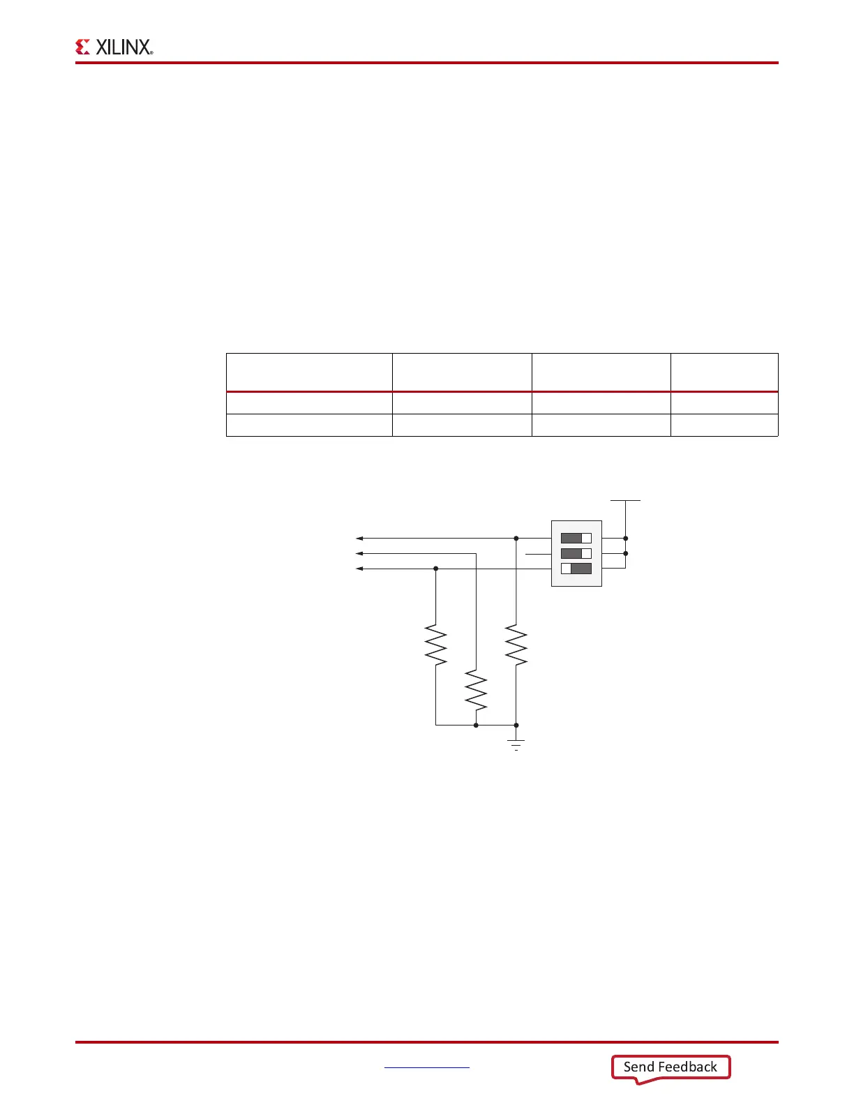
Figure 1-49 shows mode switch SW1.
Table 1-36: Mode Switch SW1 Settings
Configuration
Mode
Mode Pins (M[2:0])
Bus
Width
CCLK
Direction
Master SPI flash memory 001 x1, x2, x4 Output
JTAG 101 x1 Not applicable
X-Ref Target - Figure 1-49
Figure 1-49: Mode Switch
UG952_c1_49_030615
SDA03H1SBD
SW1
FPGA_3V3
FPGA_M0
FPGA_M2
FPGA_M1
R339
1.21K
0.1W
1%
R338
1.21K
0.1 W
1%
R337
1.21K
0.1W
1%
1
2
3
6
5
4
GND
ON
NC

 Loading...


