76 www.xilinx.com AC701 Evaluation Board
UG952 (v1.3) April 7, 2015
Chapter 1: AC701 Evaluation Board Features
For external measurements, an XADC header (J19) is provided. This header can be used to
provide analog inputs to the FPGA dedicated VP/VN channel, and to the VAUXP[0]/
VAUXN[0], VAUXP[8]/VAUXN[8] auxiliary analog input channels. Simultaneous
sampling of Channel 0 and Channel 8 is supported.
A user-provided analog signal multiplexer card can be used to sample additional external
analog inputs using the four GPIO pins available on the XADC header as multiplexer
address lines.
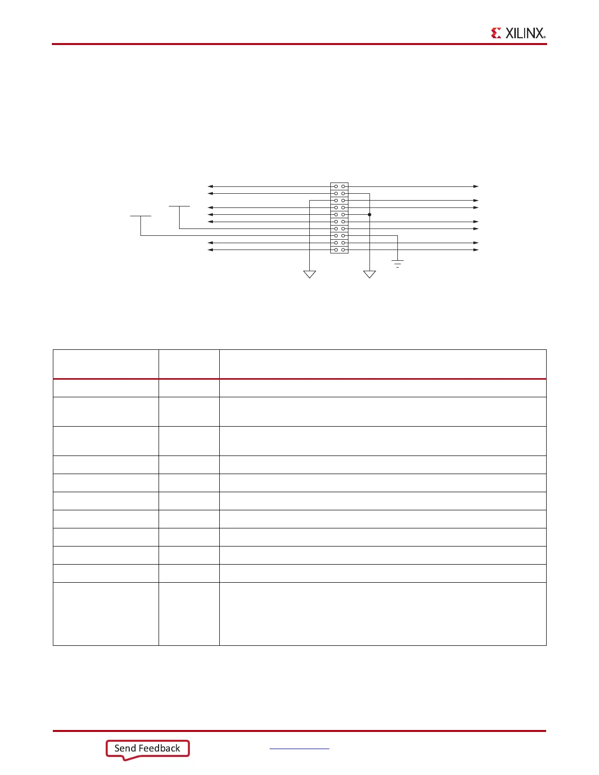
Figure 1-48 shows the XADC header J19 connections.
Table 1-35 describes the XADC header J19 pin functions.
X-Ref Target - Figure 1-48
Figure 1-48: XADC header (J19)
UG952_c1_40_101612
XADC_VP
XADC_VAUX0N
XADC_VAUX8P
XADC_DXN
XADC_VCC_HEADER
XADC_VN
XADC_VAUX0P
XADC_VAUX8N
XADC_DXP
XADC_VREF
XADC_GPIO_0
XADC_GPIO_2
XADC_GPIO_1
XADC_GPIO_3
J19
1
3
5
7
9
11
13
15
17
19
2
4
6
8
10
12
14
16
18
20
GND
XADC_AGNDXADC_AGND
XADC_VCC5V0
VCCO_VADJ
Table 1-35: XADC Header J19 Pinout
Net Name
J19 Pin
Number
Description
XADC_VN, _VP 1, 2 Dedicated analog input channel for the XADC.
XADC_VAUX0P, N 3, 6
Auxiliary analog input channel 0. Also supports use as I/O inputs when anti
alias capacitor is not present.
XADC_VAUX8N, P 7, 8
Auxiliary analog input channel 8. Also supports use as I/O inputs when anti
alias capacitor is not present.
DXP, DXN 9, 12 Access to thermal diode.
XADC_AGND 4, 5, 10 Analog ground reference.
XADC_VREF 11 1.25V reference from the board.
XADC_VCC5V0 13 Filtered 5V supply from board.
XADC_VCC_HEADER 14 Analog 1.8V supply for XADC.
VCCO_VADJ 15 V
CCO
supply for bank which is the source of DIO pins.
GND 16 Digital ground (board) reference
XADC_GPIO_3, 2, 1, 0 19, 20, 17, 18
Digital I/O. These pins come from FPGA U1 banks 15 and 16
(V
CCO
= VCCO_VADJ). The XDC constraints file I/O standard is default
LVCMOS25, assuming VCCO_VADJ = 2.5V. If VCCO_VADJ is changed from
2.5V to 1.8V or 3.3V, the ADC file I/O standard for these nets needs to be
changed to match.

 Loading...


