34 www.xilinx.com AC701 Evaluation Board
UG952 (v1.3) April 7, 2015
Chapter 1: AC701 Evaluation Board Features
U4 IN0: GTP Transceiver SMA Clock Input
[Figure 1-2, callout 9]
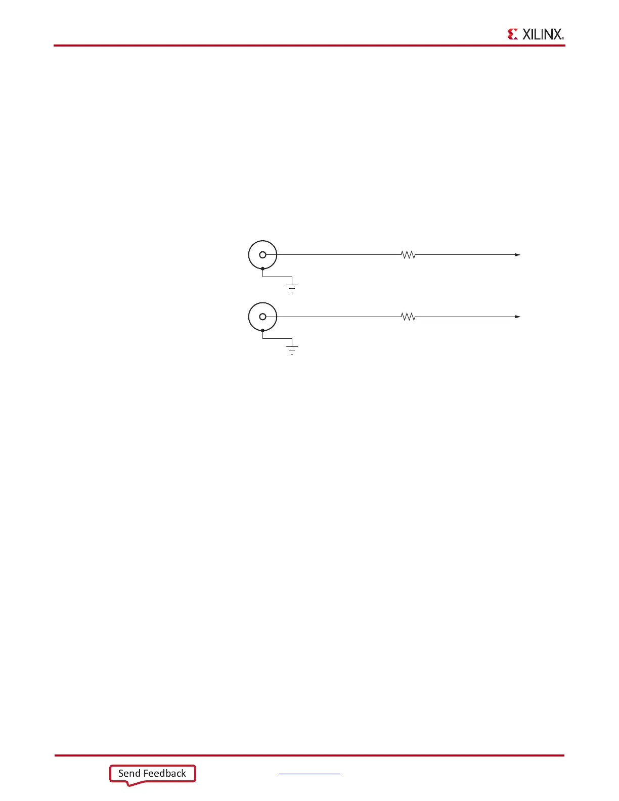
The AC701 board includes a pair of SMA connectors for a GTP transceiver clock that are
wired to GTP quad bank 213 through clock MUX U4. This differential clock has signal
names SMA_MGT_REFCLK_P and SMA_REFCLK_N, which are connected to MGT clock
MUX U4 input 0 pins 4 and 2 respectively. The clock MUX output pins 10 (P-side) and 11
(N-side) are capacitively coupled to FPGA U1 GTP Quad 213 MGTREFCLK1 pin AA11
and AB11 respectively.
Figure 1-19 shows this direct-coupled SMA clock input circuit.
• External user-provided GTP reference clock on SMA input connectors
• Differential input
U3/U4 IN2: FMC HPC GBT Clocks
[Figure 1-2, callout 29]
The FMC HPC connector J30 sources two MGT clocks. FMC1_HPC_GBTCLK0_M2C_P/N
from FMC connector section D (J30.D4(P), J30.D5(N)) is wired to SY89544UMG U3 IN2,
pins 27(P) and 25(N). FMC1_HPC_GBTCLK1_M2C_P/N from connector section B
(J30.B20(P), J30.B21(N)) is wired to SY89544UMG U4 IN2, pins 27(P) and 25(N).
GTP Transceivers
[Figure 1-2, callout 11]
The AC701 board provides access to eight GTP transceivers:
• Four of the GTP transceivers are wired to the PCI Express x4 endpoint edge connector
(P1) fingers
• Two of the GTP transceivers are wired to the FMC HPC connector (J30)
• One GTP transceiver is wired to SMA connectors (RX: J46, J47 TX: J44, J45)
• One GTP transceiver is wired to the SFP/SFP+ Module connector (P3)
X-Ref Target - Figure 1-19
Figure 1-19: GTP SMA Clock Source
UG952_c1_14_101512
SMA_MGT_REFCLK_PSMA_MGT_REFCLK_C_P
SMA
Connector
J25
GND
R485
0Ω 5%
0Ω 5%
SMA_MGT_REFCLK_NSMA_MGT_REFCLK_C_N
SMA
Connector
J26
GND
R484

 Loading...


