AC701 Evaluation Board www.xilinx.com 35
UG952 (v1.3) April 7, 2015
Feature Descriptions
The GTP transceivers in 7 series FPGAs are grouped into four channels described as
Quads. The reference clock for a Quad can be sourced from the Quad above or Quad below
the GTP Quad of interest. There are two GTP transceiver Quads on the AC701 board with
connectivity as shown here:
• Quad 213
• Contains four GTP transceivers:
- GTP0 SFP
- GTP1 FMC HPC DP0
- GTP2 FMC HPC DP1
- GTP3 SMA transmit/receive connector pairs
• MGTREFCLK0 Clock MUX U3 output
• MGTREFCLK1 Clock MUX U4 output
• Quad 216
• Contains four GTP transceivers for PCIe lanes 0–3
• MGTREFCLK0 PCIe edge connector clock
•MGTREFCLK1 NC
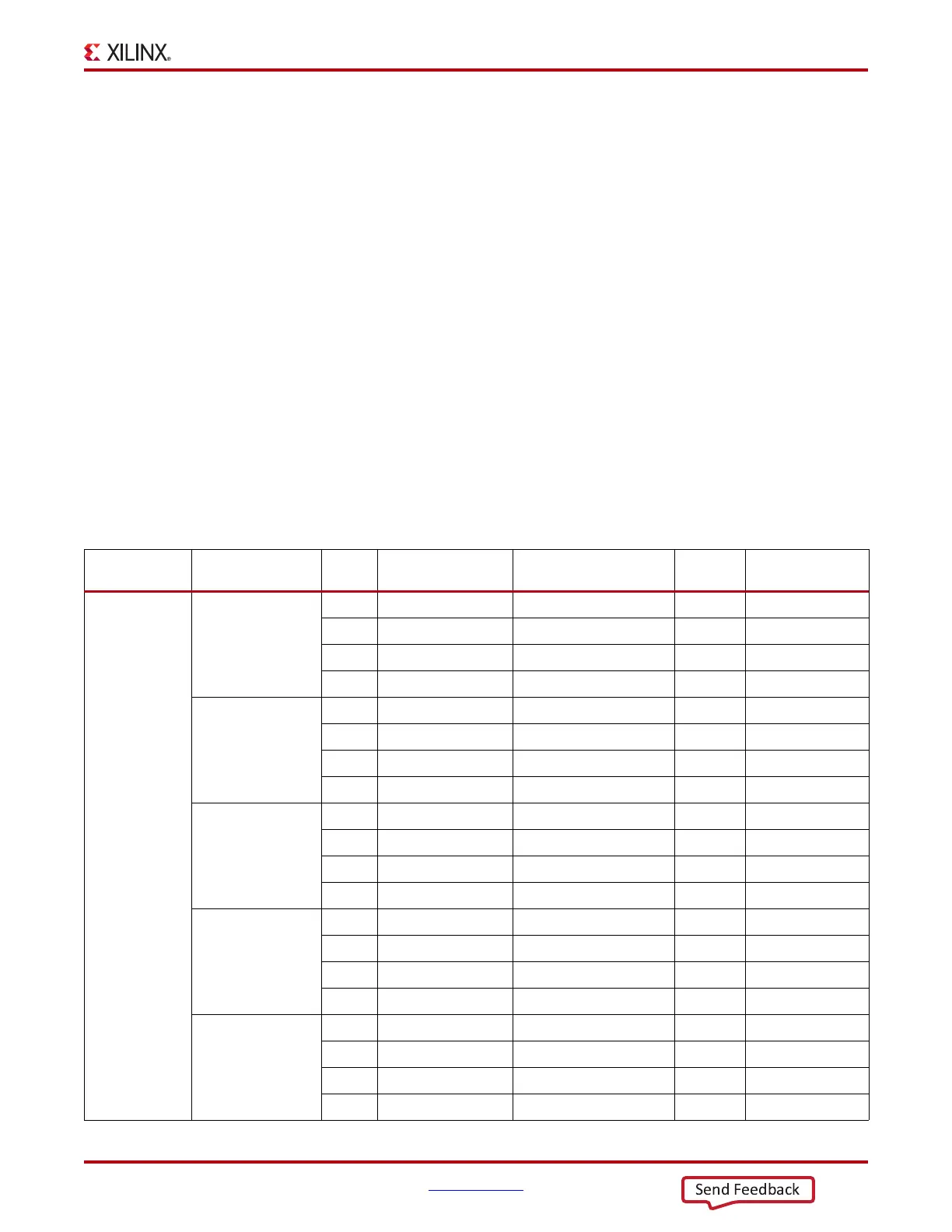
Table 1-12 lists the GTP transceiver interface connections to the FPGA (U1).
Table 1-12: GTP Transceiver Interface Connections for FPGA U1
Transceiver Bank Placement
Pin
Number
Pin Name Schematic Net Name
Connected
Pin
Connected Device
GTP_BANK_213 GTPE2_CHANNEL_
X0Y0
AC10 MGTPTXP0_213 SFP_TX_P P3.18 SFP+ Conn. P3
AD10 MGTPTXN0_213 SFP_TX_N P3.19 SFP+ Conn. P3
AC12 MGTPRXP0_213 SFP_RX_P P3.13 SFP+ Conn. P3
AD12 MGTPRXN0_213 SFP_RX_N P3.12 SFP+ Conn. P3
GTPE2_CHANNEL_
X0Y1
AE9 MGTPTXP1_213 FMC1_HPC_DP0_C2M_P J30.C2 FMC HPC J30
AF9 MGTPTXN1_213 FMC1_HPC_DP0_C2M_N J30.C3 FMC HPC J30
AE13 MGTPRXP1_213 FMC1_HPC_DP0_M2C_P J30.C6 FMC HPC J30
AF13 MGTPRXN1_213 FMC1_HPC_DP0_M2C_N J30.C7 FMC HPC J30
GTPE2_CHANNEL_
X0Y2
AC8 MGTPTXP2_213 FMC1_HPC_DP1_C2M_P J30.A22 FMC HPC J30
AD8 MGTPTXN2_213 FMC1_HPC_DP1_C2M_N J30.A23 FMC HPC J30
AC14 MGTPRXP2_213 FMC1_HPC_DP1_M2C_P J30.A2 FMC HPC J30
AD14 MGTPRXN2_213 FMC1_HPC_DP1_M2C_N J30.A3 FMC HPC J30
GTPE2_CHANNEL_
X0Y3
AE7 MGTPTXP3_213 SMA_MGT_TX_P J44.1 Clock input SMA
AF7 MGTPTXN3_213 SMA_MGT_TX_N J45.1 Clock input SMA
AE11 MGTPRXP3_213 SMA_MGT_RX_P J46.1 Clock input SMA
AF11 MGTPRXN3_213 SMA_MGT_RX_N J47.1 Clock input SMA
GTPE2_CHANNEL_
X0Y0
AA13 MGTREFCLK0P_213 SFP_MGT_CLK0_C_P U3.10
(1)
Clock MUX U3
AB13 MGTREFCLK0N_213 SFP_MGT_CLK0_C_N U3.11
(1)
Clock MUX U3
AA11 MGTREFCLK1P_213 SFP_MGT_CLK1_C_P U4.10
(1)
Clock MUX U4
AB11 MGTREFCLK1N_213 SFP_MGT_CLK1_C_N U4.11
(1)
Clock MUX U4

 Loading...


