36 www.xilinx.com AC701 Evaluation Board
UG952 (v1.3) April 7, 2015
Chapter 1: AC701 Evaluation Board Features
For more information on the GTP transceivers see 7 Series FPGAs GTX/GTH Transceivers
User
Guide (UG476) [Ref 7].
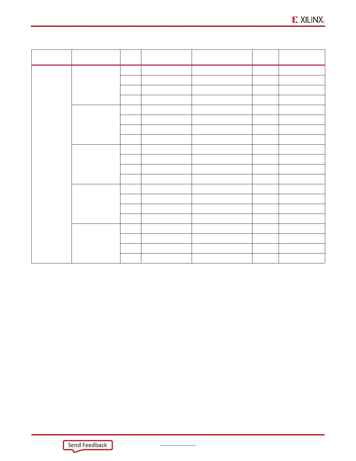
GTP_BANK_216 GTPE2_CHANNEL_
X0Y4
B7 MGTPTXP0_216 PCIE_TX3_P P1.A29
(2)
PCIe edge conn. P1
A7 MGTPTXN0_216 PCIE_TX3_N P1.A30
(2)
PCIe edge conn. P1
B11 MGTPRXP0_216 PCIE_RX3_P P1.B27 PCIe edge conn. P1
A11 MGTPRXN0_216 PCIE_RX3_N P1.B28 PCIe edge conn. P1
GTPE2_CHANNEL_
X0Y5
D8 MGTPTXP1_216 PCIE_TX2_P P1.A25
(2)
PCIe edge conn. P1
C8 MGTPTXN1_216 PCIE_TX2_N P1.A26
(2)
PCIe edge conn. P1
D14 MGTPRXP1_216 PCIE_RX2_P P1.B23 PCIe edge conn. P1
C14 MGTPRXN1_216 PCIE_RX2_N P1.B24 PCIe edge conn. P1
GTPE2_CHANNEL_
X0Y6
B9 MGTPTXP2_216 PCIE_TX1_P P1.A21
(2)
PCIe edge conn. P1
A9 MGTPTXN2_216 PCIE_TX1_N P1.A22
(2)
PCIe edge conn. P1
B13 MGTPRXP2_216 PCIE_RX1_P P1.B19 PCIe edge conn. P1
A13 MGTPRXN2_216 PCIE_RX1_N P1.B20 PCIe edge conn. P1
GTPE2_CHANNEL_
X0Y7
D10 MGTPTXP3_216 PCIE_TX0_P P1.A16
(2)
PCIe edge conn. P1
C10 MGTPTXN3_216 PCIE_TX0_N P1.A17
(2)
PCIe edge conn. P1
D12 MGTPRXP3_216 PCIE_RX0_P P1.B14 PCIe edge conn. P1
C12 MGTPRXN3_216 PCIE_RX0_N P1.B15 PCIe edge conn. P1
GTPE2_CHANNEL_
X0Y1
F11 MGTREFCLK0P_216 PCIE_CLK_QO_P P1.A13
(2)
PCIe edge conn. P1
E11 MGTREFCLK0N_216 PCIE_CLK_QO_N P1.A14
(2)
PCIe edge conn. P1
F13 MGTREFCLK1P_216 NC NA NA
E13 MGTREFCLK1N_216 NC NA NA
Notes:
1. Clock MUX U3 and U4 output nets are capacitively coupled to the GTP REFCLK input pins.
2. PCIE_TXn_P/N and PCIE_CLK_Q0_P/N are capacitively coupled to the PCIe edge connector P1.
Table 1-12: GTP Transceiver Interface Connections for FPGA U1 (Cont’d)
Transceiver Bank Placement
Pin
Number
Pin Name Schematic Net Name
Connected
Pin
Connected Device

 Loading...


