18
JOHNSON CONTROLS
FORM 201.21-NM1 (616)
PRODUCT DESCRIPTION
The power section of the drive is composed of four
major blocks consisting of an AC to DC rectier section
with accompanying pre-charge circuit, a DC link lter
section, a three phase DC to AC inverter section, and
an output suppression network.
The AC to DC rectier utilizes a semi-converter formed
by the connection of three SCR/diode modules (1SCR-
3SCR) in a three phase bridge conguration. The mod-
ules are mounted on a liquid cooled heatsink. Use of the
semi-converter conguration permits implementation
of a separate pre-charge circuit to limit the ow of cur-
rent into the DC link lter capacitors when the drive is
switched on and it also provides a fast disconnect from
the power mains when the drive is switched off. When
the drive is turned off, the SCRs in the semiconverter
remain in a non-conducting mode and the DC link lter
capacitors remain uncharged. When the drive is com-
manded to run, the DC link lter capacitors are slowly
charged via the semi-converter. The SCR’s are then
gated fully on.
Three power fuses (1FU - 3FU), an optional circuit
breaker (1SW) and a standard 5% impedance minimum
3 phase line reactor connect the AC to DC converter to
the incoming power. Very fast semiconductor power
fuses are utilized to ensure that the SCR/diode module
packages do not rupture if a catastrophic failure were to
occur on the DC link. The SCR Trigger board provides
the gating pulses for the SCR’s as commanded by the
VSD Logic board.
The DC Link lter section of the drive consists of a
group of electrolytic lter capacitors (C1-C6). This ca-
pacitor bank effectively smooths the ripple voltage from
the AC to DC rectier while simultaneously providing a
large energy reservoir for use by the DC to AC inverter
section of the drive. In order to achieve the required
voltage capability for the capacitor portion of the lter,
lter capacitor “banks” are formed by connecting two
groups of parallel capacitors in series to form a capaci-
tor “bank”. In order to assure an equal sharing of the
voltage between the series connected capacitors and to
provide a discharge means for the capacitor bank when
the VSD is powered off, “bleeder” resistors (1RES and
2RES) are connected across the capacitor banks.
The DC to AC inverter section of the VSD serves to
convert the rectied and ltered DC back to AC at the
magnitude and frequency commanded by the VSD Logic
board. The inverter section is actually composed of two
to four identical inverter output phase assemblies. These
assemblies are in turn composed of 3 pairs of Insulated
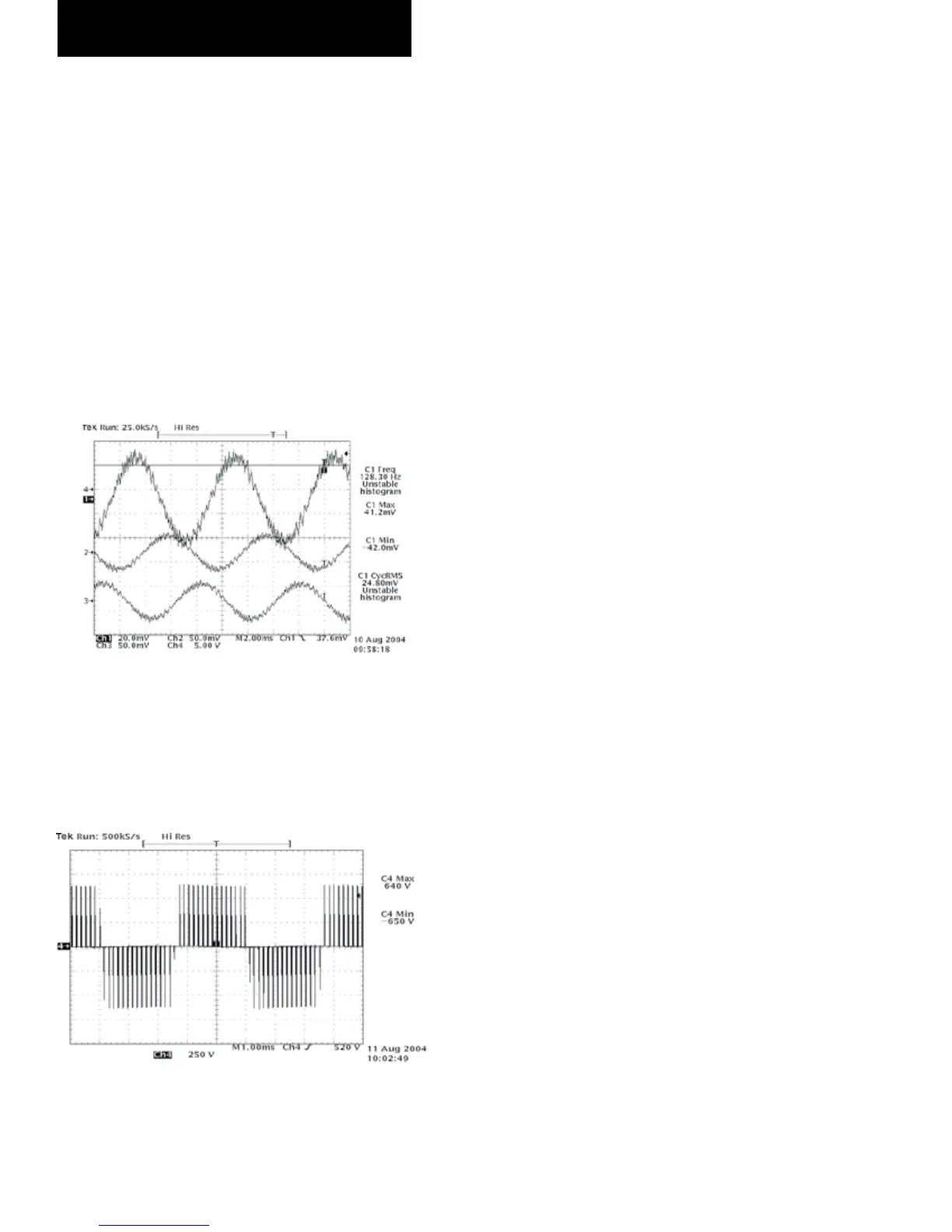
FIG. 2 - PWM VOLTAGE WAVEFORM
LD10480
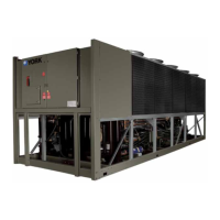
Variable Speed Drive (VSD)
The VSD (variable speed drive) is a liquid cooled, tran-
sistorized, PWM inverter, which provides speed control
to vary the speed of 2, 3 or 4 compressor motors. The
VSD changes the duration of the voltage pulses supplied
to the motor to enable control of compressor speed to
match the system load. A PWM generator, on the VSD
Logic Board, with a switching frequency of 3125 Hz
modulates the voltage signal to provide a relatively
pulses constant V/F ratio. In some cases, the V/F ratio
is slightly modied to provide additional torque to the
motor. Sample 3 phase current waveforms are shown
in FIG. 1 to show the sinusoidal characteristics of the
current drawn by the compressor motors.
FIG. 1 - PWM CURRENT WAVEFORM
LD10479
A Sample PWM voltage waveforms is shown in FIG.
2. The pulses near the sides of the rectangular groups
of waves are notably narrower, representing the lower
voltage of a sinusoidal waveform as it rises or falls from
the “0” crossing.
 Loading...