Product Principle 4-5
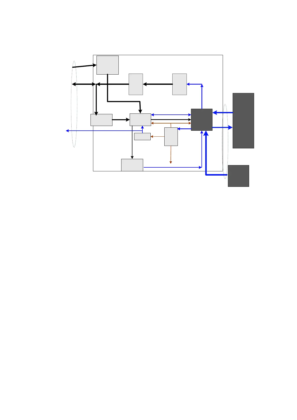
4.2.3 Front-end of Main Board
Signal
process
FPGA
Main board transmitting and receiving
High-
voltage
pulse
output
circuit
Low-
voltage
drive
circuit
ATGC
High-
voltage
isolation
AFE clip
x8
Clock
TRA
FPGA
Clock
circuit
64ch
RX,
64ch
64ch
64ch
CW
receiving
circuit
Connect to
probe via
TR 64
board
Control TR
64 board
Pencil
probe
receiving
switch
Pencil
probe
control
data
TRB
FPGA
65-128
channel
data
Transmitting
control
I/Qsignal
TX,64ch
PEN_RX
C
o
n
n
e
c
t
o
r
t
o
b
o
a
r
d
C
o
n
n
e
c
t
o
r
t
o
b
o
a
r
d
Fig 4-4 Systematical diagram of front-end of main board
The main functions of main board’s front-end unit:
Control FPGA (TRA, implements the control of 65-128 channels transmitting and receiving,
ATGC adjustment and CW receiving control).
Clock circuit
Transmitting circuit (transmits the pulse with the achievement of 5 electric levels)
High-voltage isolation
AFE (receives echo signal)
ATGC circuit (time gain compensation)
CW receiving circuit (CW signal receiving)
 Loading...