PRELIMINARY INFORMATION
NVIDIA Jetson Orin NX DG-10931-001_v0.1 | 13
Chapter 6. Power
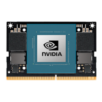
Power for the module is supplied on the VDD_IN pins and is nominally 5.0V to 20V (see the
Jetson Orin NX Data Sheet
for supply tolerance and maximum current).
CAUTION: Jetson Orin NX is not hot-pluggable. Before installing or removing the module, the
main power supply (to VDD_IN pins) must be disconnected and adequate time allowed for the
various power rails to fully discharge.
Table 6-1. Jetson Orin NX Power and System Pin Description
Pin #
Module Pin
Name
Orin Pin Name Usage and Description
Recommended
Usage
Direction Pin Type
251
260
VDD_IN − Main power – Supplies PMIC and other
regulators
Main DC input Input 5.0V to 20V
235 PMIC_BBAT − Real-Time-Clock back-up. Optionally used to
provide back-up power for the RTC in the Power
Sequencer. Connects to a Lithium Cell or
similar power source. The cell sources power
for the RTC when system is disconnected from
power.
Battery Back-up
using coin cell,
etc..
Input 1.75V to
5.5V
214 FORCE_
RECOVERY*
GP107_
RECOVERY0_ST
RAP
Force Recovery strap pin. Held low when
SYS_RESET* goes high (i.e. during power-on)
places system in USB recovery mode. 10kΩ pull-
up to 1.8V on the module.
System Input CMOS –
1.8V
240 SLEEP/WAKE* GPO4 Sleep/Wake. Configured as GPIO for optional
use to indicate the system should enter or exit
sleep mode. 100kΩ pull-up to 1.8V on the
module.
System Input CMOS –
5.0V
233 SHUTDOWN_
REQ*
− When driven/pulled low by the module, requests
the carrier board to shut down. ~5kΩ pull-up to
VDD_IN on the module.
System Output Open
Drain,
VDD_IN
level
237 POWER_EN −
Signal for module on/off: high level on, low level
off. Connects to module PMIC EN0 through
converter logic. POWER_EN is routed to a
Schmitt trigger buffer on the module. A 100kΩ
pulldown is on the module.
System Input
Analog
5.0V
239 SYS_RESET* − Module Reset. Reset to the module when driven
low by the carrier board. Used as carrier board
System Bidir Open
Drain, 3.3V
 Loading...
