Display
PRELIMINARY INFORMATION
NVIDIA Jetson Orin NX DG-10931-001_v0.1 | 47
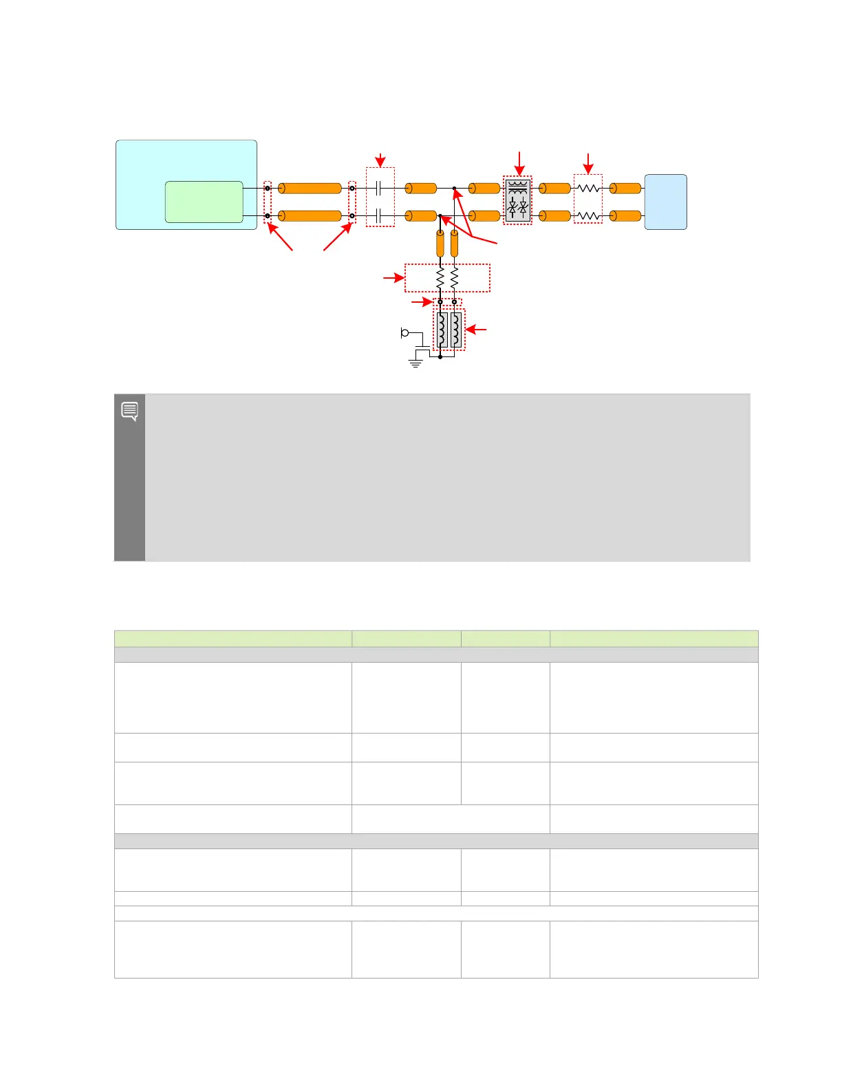
Figure 9-9. HDMI CLK and Data Topology
100Ω*
100Ω*
100Ω*
100Ω*
100Ω*
100Ω*
Jetson
HDMI
Conn
AC
C AP
Se g D Se g F
MOD_SL EEP*
49 9Ω,
1%
PCB Vias
PCB Vias
0. 1u F
0. 1u F
R
PD
Common Mode
Chokes & ES D
Se e No te 1
49 9Ω,
1%
Se g B Se g E
Se g C
SoC
95-100Ω 100Ω*
95-100Ω 100Ω*
Main Ro ute –
Se g A
* Note 3 * Note 3* Note 3 * Note 3
R
S
(See Not e 4 )
Choke or Trace
Se e No te 2
Notes:
1. RPD pad must be on the main trace. RPD and ACCAP must be on same layer.
2. Chokes (600 Ω @ 100 MHz) or narrow traces (1 uH @ DC-100 MHz) between pull-downs and
FET are chokes between pull-downs and FET are optional improvements for HDMI 2.0
operation.
3. The trace after the main route via should be routed on the top or bottom layer of the PCB,
and either with 100 ohm differential impedance, or as uncoupled 50 ohm SE traces.
4.
See the RS section in Table 9-5 for details.
Table 9-5. HDMI Interface Signal Routing Requirements
<= 2
<= 3
< 4.3
dB @ 1.5GHz
dB @ 3GHz
dB @ 6GHz
For HDMI 2.0, 6 dB and 6 GHz is
supported.
10%-90%. If TDR dip is 75~85 ohm that
dip width should < 250 ps
<= -40
dB at 3GHz
PSNEXT is derived from an algebraic
summation of the individual NEXT effects
on each pair by the other pairs
IL/FEXT plot: See HDMI Guideline
Figure 9-9
TDR plot: See Figure 9-11
Trace impedance: Diff pair
±10%. Target is 100Ω. 95Ω for the
breakout and main route is an
Trace spacing/Length/Skew
Trace loss characteristic:
< 0.8
< 0.4
dB/in. @ 3GHz
dB/in. @ 1.5GHz
The max length (delay) is derived based
on this characteristic. The length (delay)
constraint must be re-defined if the loss
characteristic is changed. See Note 1.

 Loading...