Miscellaneous Interfaces
PRELIMINARY INFORMATION
NVIDIA Jetson Orin NX DG-10931-001_v0.1 | 69
12.6 Debug
Jetson Orin NX supports a UART for debugging purposes. The UART intended for debug is
UART2.
Table 12-13. Jetson Orin NX Debug UART Pin Descriptions
Pin #
Module Pin
Name Orin Signal Usage and Description
Recommended
Usage Direction Pin Type
238 UART2_RXD GP11_UART3_TXD UART 2 receive
Debug UART
Input CMOS – 1.8V
236 UART2_TXD GP12_UART3_RXD UART 2 transmit Output
Note: In the Direction column, Output is from Jetson Orin NX. Input is to Jetson Orin NX. Bidir is for Bidirectional signals.
Table 12-14. Debug UART Connections
Module Pin Name Type Termination Description
UART2_TXD O UART #2 Transmit: Connect to RX pin of serial device
UART2_RXD I If level shifter implemented,
100kΩ to supply on the non-
Jetson Orin NX side of the device.
UART #2 Receive: Connect to TX pin of serial device
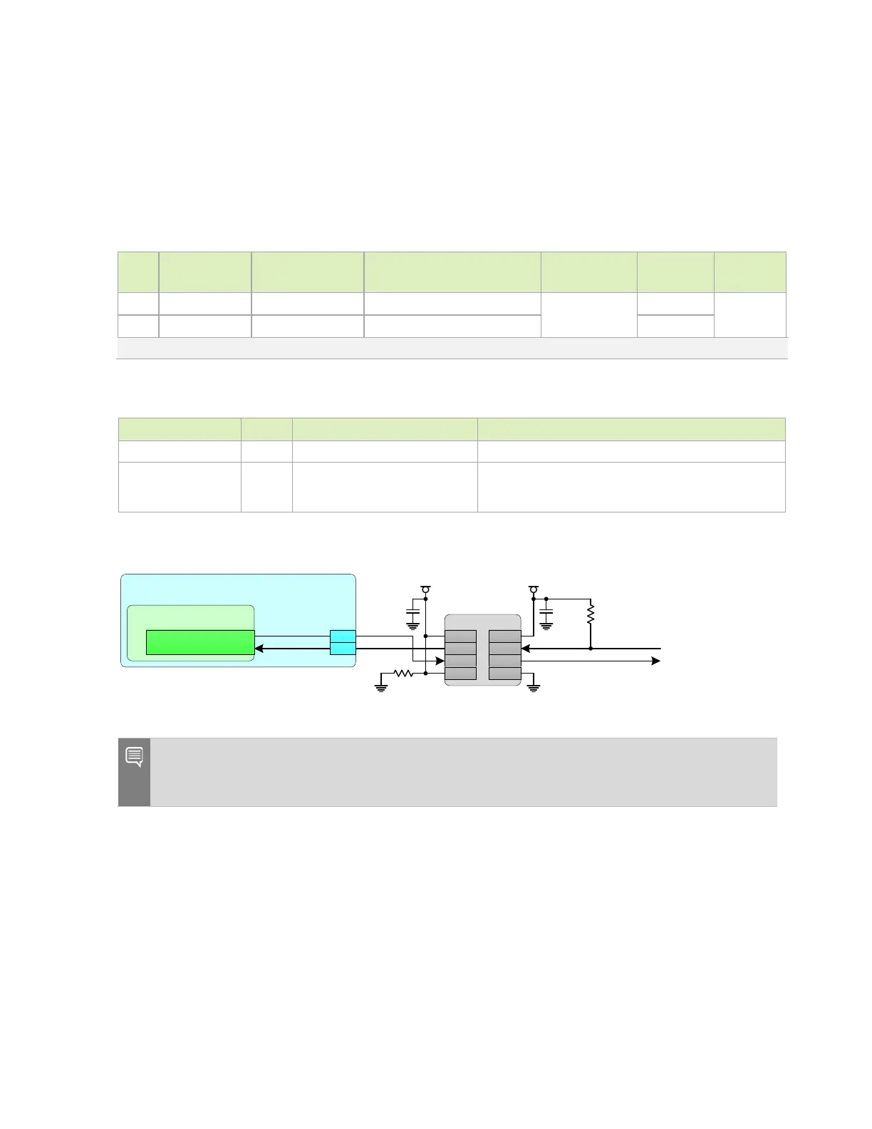
Figure 12-8. Debug UART Connections
Jetson
SoC
Level Shifter
VCCB
VCCA
B1
A1
B2A2
GNDOE
10 0k Ω
VDD_3V 3_SYSVDD_1V8
0.1uF
0.1uF
UART2_TXD
UART2_RXD
236
238
10 0k Ω
RXD_LS
TXD_L S
GP11_UART3_TXD
GP12_UART3_RXD
Note: If level shifter is implemented, pull-up is required on the RXD line on the non-Jetson Orin
NX side of the level shifter. This is required to keep the input from floating and toggling when no
device is connected to the debug UART.

 Loading...