Miscellaneous Interfaces
PRELIMINARY INFORMATION
NVIDIA Jetson Orin NX DG-10931-001_v0.1 | 65
12.2.1 SPI Design Guidelines
The following guidelines meet the SPI design guidelines.
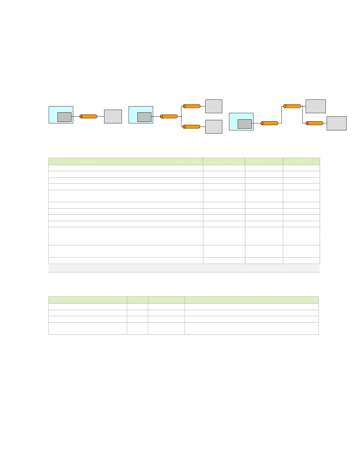
Figure 12-4. SPI Topologies
Jetson
SPI
Device
#1
Main trunk
SPI
Device
#2
SPI
Device
#1
Main trunk
SPI
Device
#2
Branch-A
Branch-B
Branch-A
Branch
-B
2x-Load Star Topology 2x-Load Daisy Topology
SPI
Device
Main trunk
SoC
Jetson
SoC
Jetson
SoC
Point-Point Topology
Table 12-5. SPI Interface Signal Routing Requirements
Configuration / device organization
Max loading (total of all loads)
Breakout region impedance
Minimum width
and spacing
Via proximity (signal to reference)
Trace spacing: Microstrip / Stripline
Max trace length/delay (PCB main trunk) For MOSI, MISO, SCK and CS
Point-point
195 (1228)
mm (ps)
Max trace length/delay (Branch-A) for MOSI, MISO, SCK and CS
2x-load star/daisy
Max trace length/delay skew from MOSI, MISO and CS to SCK
Note: Up to four signal vias can share a single GND return via
Table 12-6. SPI Signal Connections
Module Pin Names (Function)
SPI Clock.: Connect to peripheral CLK pins
SPI Data Output: Connect to target peripheral MOSI pins
SPI Data Input: Connect to target peripheral MISO pins
SPI Chip Selects.: Connect one CSx* pin per SPI interface to
each target peripheral CS pin on the interface

 Loading...