Miscellaneous Interfaces
PRELIMINARY INFORMATION
NVIDIA Jetson Orin NX DG-10931-001_v0.1 | 66
12.3 UART
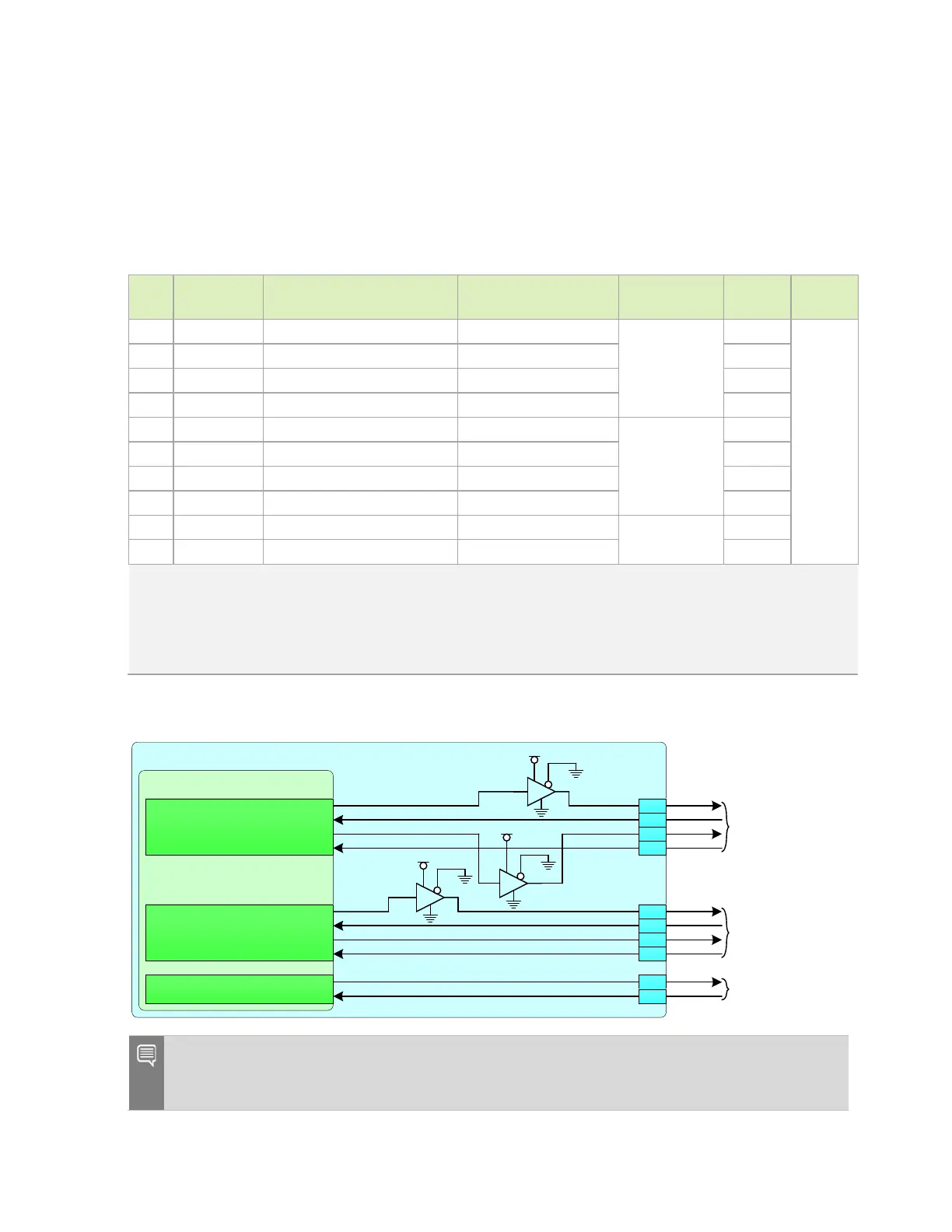
The Jetson Orin NX brings three UARTs out to the main connector. See Figure 11 5 for typical
assignments of the three available UARTs.
Table 12-7. Jetson Orin NX UART Pin Descriptions
Pin #
Module Pin
Name Orin Signal Usage and Description
Recommended
Usage Direction Pin Type
99 UART0_TXD GP32_UART2_TXD UART 0 Transmit
UART general
(i.e. M.2 Key E)
Output
CMOS –
1.8V
101 UART0_RXD GP33_UART2_RXD UART 0 Receive Input
103 UART0_RTS* GP34_UART2_RTS_N UART 0 Request to Send Output
105 UART0_CTS* GP35_UART2_CTS_N UART 0 Clear to Send Input
203 UART1_TXD GP70_UART1_TX_BOOT2_STRAP UART 1 Transmit
UART general
Output
205 UART1_RXD GP71_UART1_RXD UART 1 Receive Input
207 UART1_RTS* GP72_UART1_RTS_N UART 1 Request to Send Output
209 UART1_CTS* GP73_UART1_CTS_N UART 1 Clear to Send Input
236 UART2_TXD GP11_UART3_TXD UART 2 Transmit.
Debug UART
Output
238 UART2_RXD GP12_UART3_RXD UART 2 Receive Input
Notes:
1. In the Direction column, Output is from Jetson Orin NX. Input is to Jetson Orin NX. Bidir is for Bidirectional signals.
2. The direction indicated for the UART pins except for is true when used for that function. Otherwise, these pins support GPIO
functionality and most can support both input and output (bidirectional) functionality. The exception is UART0_TXD, UART0_RTS*
and UART1_TXD. These have output-only buffers on the module to keep them from being affected by connected devices during
boot as they are associated with SoC strapping pins.
Figure 12-5. Jetson Orin NX UART Connections
Jetson
SoC – UART
GP70_UART1_TXD_BOOT2_STRAP
GP71_UART1_RXD
GP72_UART1_RTS_N
GP73_UART1_CTS_N
D ebu g UA RT
UART0_TXD
UART0_RXD
UART0_RTS*
UART0_CTS*
UART1_TXD
UART1_RXD
UART1_RTS*
UART1_CTS*
UART2_TXD
UART2_RXD
GP11_UART3_TXD
GP12_UART3_RXD
GP32_UART2_TXD
GP33_UART2_RXD
GP34_UART2_RTS_N
GP35_UART2_CTS_N
205
203
236
238
101
99
103
105
207
209
UART general
UART general (i.e.
M. 2 Key E)
GND
OE*
VCC
GND
OE*
VCC
GND
OE*
VCC
1.8V
1.8V
1.8V
Note: The buffers on UART0_TXD, UART0_RTS* and UART1_TXD are there to prevent connected
devices from changing the pin state during power-on. These pins are associated with SoC
Strapping pins

 Loading...