USB and PCIe
PRELIMINARY INFORMATION
NVIDIA Jetson Orin NX DG-10931-001_v0.1 | 28
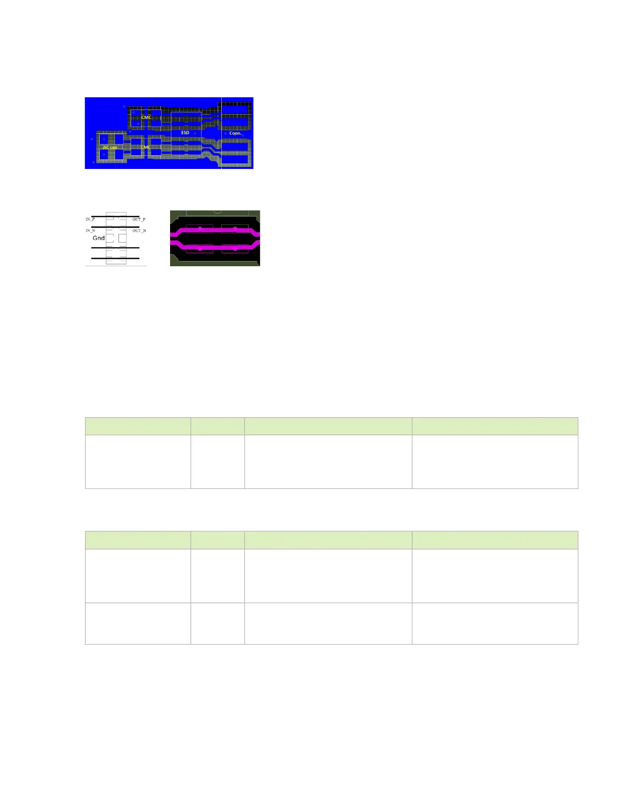
Figure 7-7. Component Placement
Figure 7-8. ESD Layout Recommendations
7.1.2.1 Common USB Routing Guidelines
If routing to USB device or USB connector includes a flex or 2nd PCB, the total routing
including all PCBs and flexes must be used for the max trace and skew calculations.
Keep critical USB related traces away from other signal traces or unrelated power traces and
areas or power supply components.
Table 7-6. Orin USB 2.0 Signal Connections
Module Ball Name Type Termination Description
USB[2:0]_D_P
USB[2:0]_D_N
DIFF I/O If used, 90Ω common-mode chokes
close to connector. ESD Protection
between choke and connector on each
line to GND
USB Differential Data Pair: Connect
to USB connector, Mini-Card socket,
hub, or another device on the PCB.
Table 7-7. Miscellaneous USB 2.0 Signal Connections
Module Pin Name Type Termination Description
GPIO00
(USB_VBUS_EN0)
I/O USB0 VBUS Enable: Connect to
enable and overcurrent pins of load
switch (through 100ohm series
resistor to OC pin).
GPIO (VBUS Detect) I 5V to 1.8V level shifter VBUS Detect: Connect to VBUS pin of
USB connector receiving USB0_+/–
interface through level shifter.

 Loading...