Smart Module Series
SG368Z_Series_Hardware_Design 43 / 113
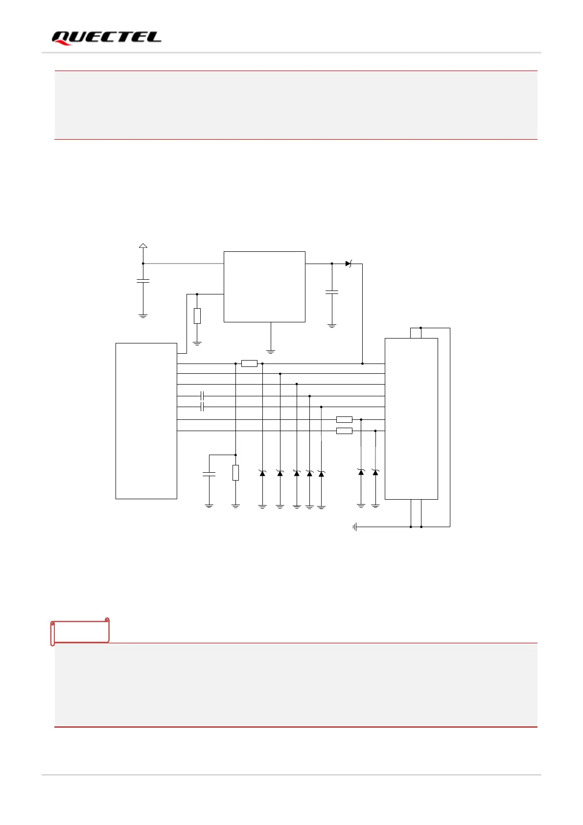
4.1.2. USB Type-A Interface
The reference design of USB Type-A interface realized by USB0 is shown below:
EN
VIN
5V_OUT
GND
10K
USB0_DP
USB0_DM
USB0_VBUS
1
2
3
9
8
USB_DP
USB_DM
VBUS
GND
GND
GND
GND
4
7
10
15K
Module
HOST_PWR_EN
VIN
C1
C2
POWER IC
R1
Schottky
10K
R2
R3
100 nF
C3
USB0_SS_TX_P
USB0_SS_TX_M
USB0_SS_RX_P
USB0_SS_RX_M
SS_TX_P
SS_TX_M
SS_RX_P
SS_RX_M
Type-A
C4
C5
100 nF
100 nF
0R
0R
R4
R5
6
5
11
Figure 9: Reference Design of USB Type-A Interface
.
design.
2. The Schottky diode in the above figure is used for anti-backflow, which will affect the VBUS output
power supply capability. If there is a high requirement for power supply capability, it is
recommended to choose a power chip that supports anti-backflow.
1. USB Type-C design requires an external CC logic chip and an SS channel switch. For details, see
document [3].
2. The Type-A design of USB1, USB2, and USB3 interfaces can refer to the above figure. It should be
noted that the module does not have corresponding VBUS and USB_ID. For external VBUS 5 V
output enable control pin, you can choose HOST_PWR_EN, or choose other GPIO.
 Loading...