– 14 –
THEORY OF OPERATION
2. Main Logic Board
2-1. Data Input Operation
2-1-1. Parallel Interface
Communications between the host computer and this printer are facilitated via parallel connectors. This section explains
the handshake of this interface.
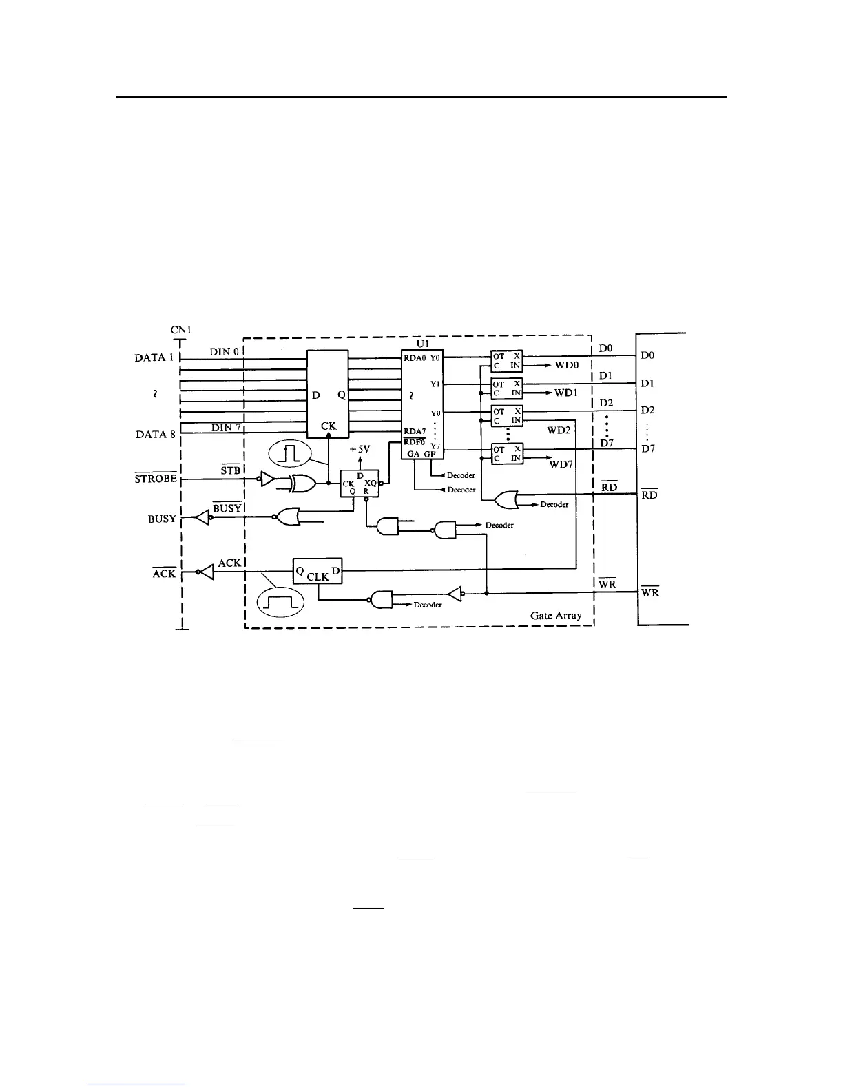
The data input circuit of this interface is shown in Fig. 2-2.
Fig. 2-2 Data Input Circuit with Parallel Interface
The following is an explanation of this handshake.
(1) When the BUSY signal is LOW (Ready), the host computer outputs 8-bit data 1 through 8 to the connector CN1.
Pin 1 carries the STROBE pulse signal from the host computer to the printer.
This signal is normally held HIGH by the host computer. When the host computer has data ready for the printer,
it sets this signal to LOW for at least 0.5 µS.
(2) The gate array of the main logic board reads data 1 through 8 at the time of STROBE signal fall, and then turns the
BUSY and RDF0 (in the device U1) signals to low.
(3) When the BUSY signal of the gate array is set to LOW, the BUSY signal of connector CN1 will be turned to HIGH,
notifying the host computer that data cannot be accepted.
(4) The CPU is informed via the D0 data line that the RDF0 signal is LOW. The CPU then, set the RD signal to LOW
and read the data.
(5) Upon completion of the data reading, the CPU notifies the host computer of the data receivable state by setting the
BUSY signal of connector CN1 and the ACK signal to LOW for a certain period of time.
This concludes the explanation of the parallel interface handshake. The following chart shows the timing chart of
the handshake.