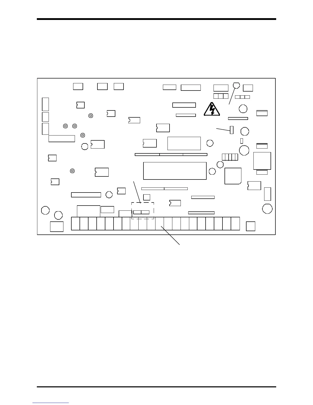
4.6 Control Board for G2+2270 through G2+2330 and
G2+4270 through G2+430K
The following pictorial shows a layout of the major components located on the
control board VF3C-1200.
4 - 9
CN20
CN3CN2CN11
See Detail 2
Page 4-11
JP1 JP2
CN10
FL-RY
CN7
See Terminal Block Detail
Page 4-11
CN8
CN1
CN4
CN5CN6
CN4B
CN4A
CN4C
CP4
CP1
CP2
CP5
CP3
CN12
Note:
1) CP1, CP2, CP3, CP4, and CP5 are service testpoints.
2) Do not adjust JP4.
3) Charge LED indicates charged capacitors. DO NOT TOUCH internal parts if lighted.
TOSHIBA
Charge
LED
JP4
Do Not
Adjust
 Loading...