AC701 Evaluation Board www.xilinx.com 13
UG952 (v1.3) April 7, 2015
Feature Descriptions
For full details on configuring the FPGA, see 7 Series FPGAs Configuration User Guide
(UG470)
[Ref 5].
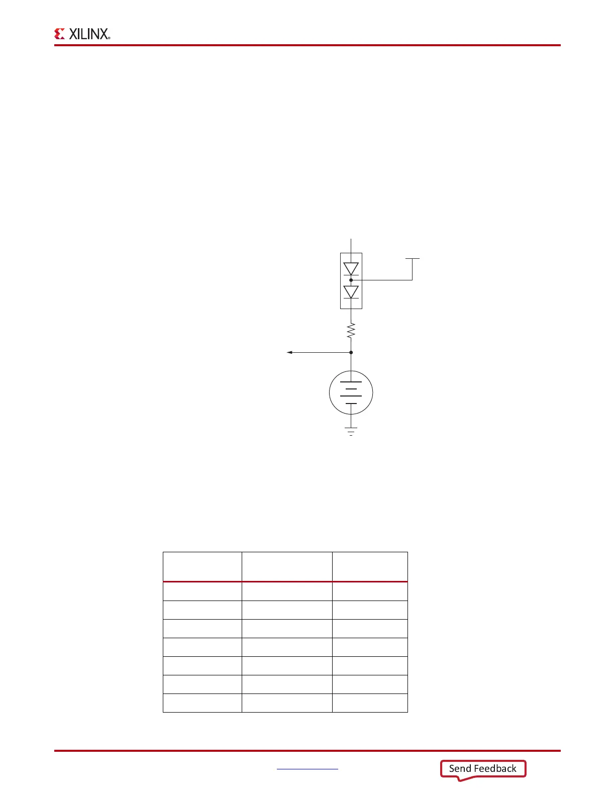
Encryption Key Backup Circuit
FPGA U1 implements bitstream encryption key technology. The AC701 board provides the
encryption key backup battery circuit shown in
Figure 1-4. The rechargeable 1.5V lithium
button-type battery B1 is soldered to the board with the positive output connected to
FPGA U1 VCCBATT pin G14. The battery supply current I
BATT
specification is 150 nA
maximum when board power is off. B1 is charged from the VCC1V8 1.8V rail through a
series diode with a typical forward voltage drop of 0.38V and 4.7 kΩ current limit resistor.
The nominal charging voltage is 1.62V.
I/O Voltage Rails
In addition to Bank 0, there are eight I/O banks available on the Artix-7 device. The
voltages applied to the FPGA I/O banks used by the AC701 board are listed in
Table 1-3.
X-Ref Target - Figure 1-4
Figure 1-4: Encryption Key Backup Circuit
UG952_c1_04_092812
GND
2
2
1
1
B1
1.5V
Seiko
TS518SE_FL35E
2
1
3
BAS40-04
D6
40V
200 mW
NC
FPGA_VBATT
+
VCC1V8 (1.8V)
R83
4.70K 5%
1/10W
Table 1-3: FPGA Bank Voltage Rails
U1 FPGA Bank
Power Supply Rail
Net Name
Voltage
Bank 0 FPGA_3V3 3.3V
Bank 12 VCCO_VADJ 2.5V
Bank 13 FPGA_1V8 1.8V
Bank 14 FPGA_3V3 3.3V
Bank 15 VCCO_VADJ 2.5V
Bank 16 VCCO_VADJ 2.5V
Bank 33 FPGA_1V5 1.5V

 Loading...


