30 www.xilinx.com AC701 Evaluation Board
UG952 (v1.3) April 7, 2015
Chapter 1: AC701 Evaluation Board Features
Clock Multiplexer U4 SY89544UMG drives Bank 213 MGTREFCLK1 pins AA11 (P) and
AB11(N). See
Table 1-11 for clock Multiplexer U4 connections.
The Multiplexer U4 clock input channel select nets are PCIE_MGT_CLK_SEL[1:0].
Net PCIE_MGT_CLK_SEL1 is wired to FPGA U1 pin C26 and net PCIE_MGT_CLK_SEL0
is wired to FPGA U1 pin A24 on FPGA U1 Bank 16.
The U4 Multiplexer circuit is shown in Figure 1-16.
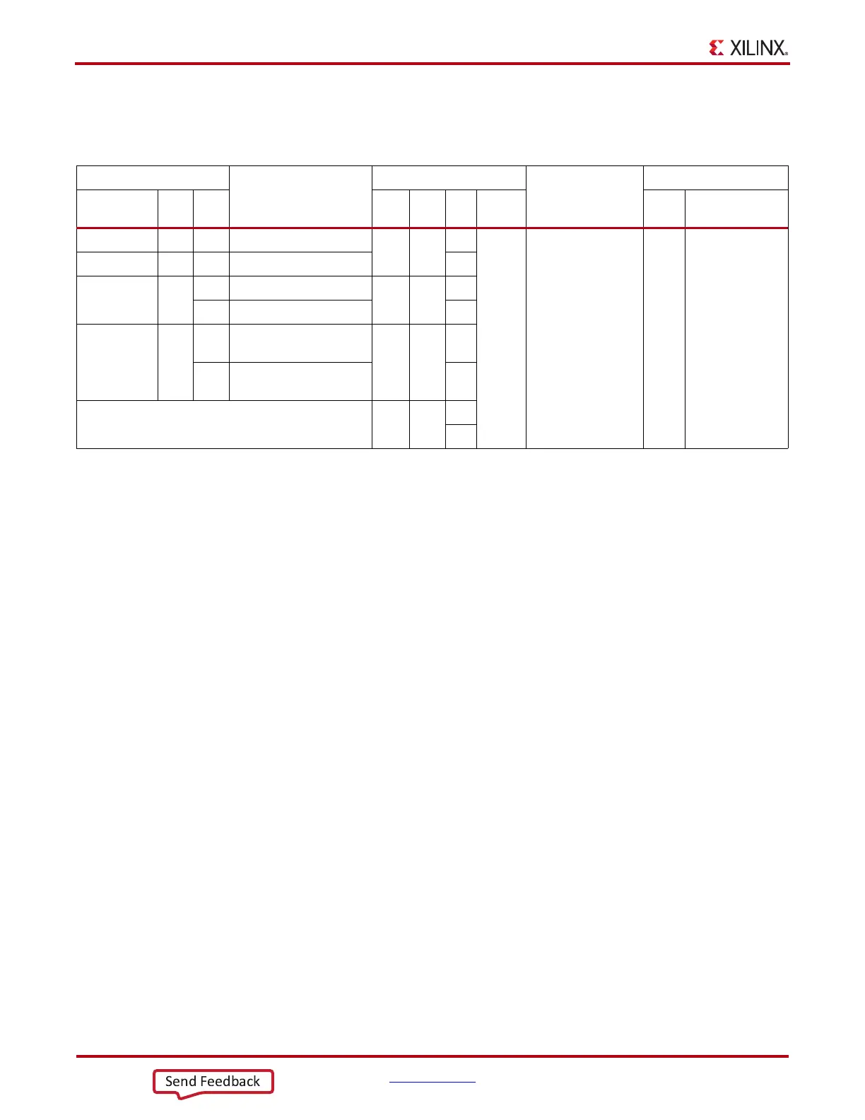
Table 1-11: Multiplexer U4 SY89544UMG MGT Clock Inputs
Clock Source
Schematic Net Name
SY89544UMG (U4)
Schematic Net Name
(1)
FPGA U1 Bank 213
Device Ref Pin Input
SEL
[1:0]
Pin Output Pin Pin Name
SMA J25 1 SMA_MGT_REFCLK_P
IN0 00
4
10(Q)
11(QB)
SFP_MGT_CLK1_P
SFP_MGT_CLK1_N
AA11
AB11
MGTREFCLK1P
MGTREFCLK1N
SMA J26 1 SMA_MGT_REFCLK_N 2
SI5324C-GM U24
35 SI5324_OUT1_C_N
IN1 01
32
34 SI5324_OUT1_C_P 30
FMC HPC J30
B20
FMC1_HPC_
GBTCLK1_M2C_P
IN2 10
27
B21
FMC1_HPC_
GBTCLK1_M2C_N
25
Not connected IN3 11
23
21
Notes:
1. U4 output clock nets SFP_MGT_CLK0_P/N implement a series 0.1 μF capacitor.
2. SEL[1:0] nets PCIE_MGT_CLK_SEL1 FPGA U1 pin C26 and PCIE_MGT_CLK_SEL0 FPGA U1 pin A24
I/O standard = LVCMOS25 (IOSTANDARD assumes default V
ADJ
of 2.5V)

 Loading...


