AC701 Evaluation Board www.xilinx.com 65
UG952 (v1.3) April 7, 2015
Feature Descriptions
VCCO_VADJ Voltage Control
The FMC VCCO_VADJ rail is set to 2.5V. When the AC701 board is powered on, the state
of the FMC_VADJ_ON_B signal wired to header J8 is sampled by the TI UCD90120A
controller U9. If a jumper is installed on J8, signal FMC_VADJ_ON_B is held low, and TI
controller U9 energizes the FMC VCCO_VADJ rail at power on.
Removing the jumper at J8 after the board is powered up does not affect the 2.5V power
delivered to the VCCO_VADJ rail and it remains on.
A jumper installed at J8 is the default setting. If a jumper is not installed on J8 at power on,
the signal FMC_VADJ_ON_B is High and the AC701 board does not energize the
VCCO_VADJ 2.5V power.
Installing a jumper at J8 after the AC701 board powers up in this mode turns on the
VCCO_VADJ rail.
In this VCCO_VADJ off mode, you can control when to turn on VCCO_VADJ and to what
voltage level (1.8V, 2.5V or 3.3V).
With VCCO_VADJ off, the FPGA still configures and has access to the TI controller PMBus
and the VADJ_ON_B signal which are wired to FPGA U1 Bank 14. The combination of
these features allows you to develop code to command the VCCO_VADJ rail to be set to
1.8V or 3.3V instead of the default setting of 2.5V.
See AC701 board schematic page 46 for a brief discussion concerning selectable
VCCO_VADJ voltages. The important controller-to-regulator circuit signals are
VCCO_VADJ_EN and FMC_ADJ_SEL[1:0]. In the VCCO_VADJ off mode, controller U9
does not toggle the regulator turn-on signal VCCO_VADJ_EN High, so the U56 regulator
stays off. You must re-program the controller U9 VCCO_VADJ rail settings to the desired
VCCO_VADJ voltage so that the controller expects the new voltage to appear on its MON1
remote sense pin. The FMC_ADJ_SEL[1:0] controller GPIO16 and GPIO17 pins must be set
to the correct logic levels to force the VCCO_VADJ regulator Reset MUX U64 to select the
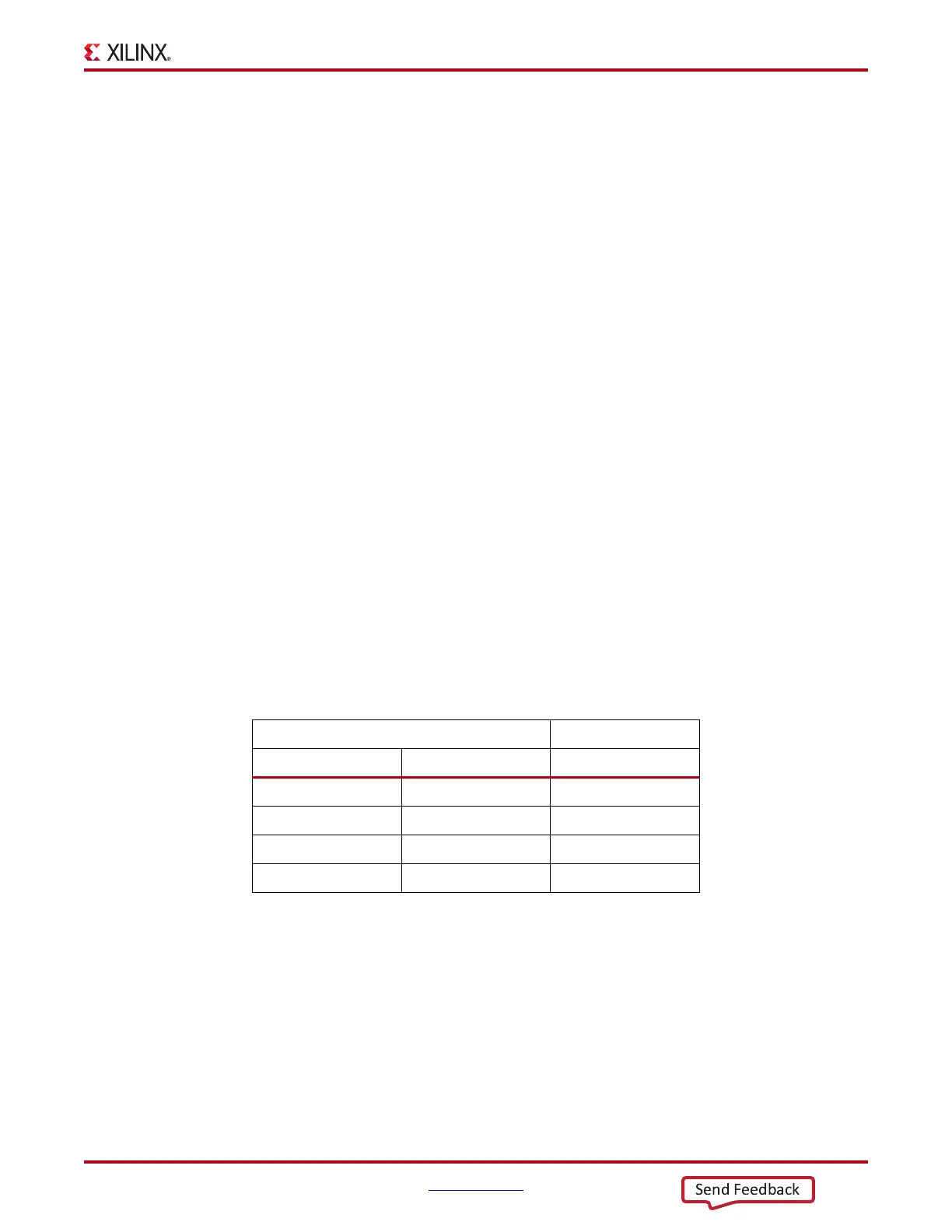
appropriate RT_CLK and VADJ resistors for the desired voltage as shown in
Table 1-30.
When the new VCCO_VADJ rail settings and Reset MUX logic levels are programmed into
controller U9, the FMC_VADJ_ON_B signal can be driven Low by user FPGA logic and the
controller toggles the VCCO_VADJ_EN signal High to allow the rail to come up at the new
VCCO_VADJ voltage level.
Documentation describing PMBus programming for the UCD90120A controller is
available at Texas Instruments
[Ref 22].
Table 1-30: VCCO_VADJ Voltage Selection
FMC_ADJ_SEL[10] VCCO_ADJ (V)
BIT 1 BIT 0
0 0 2.5V
0 1 1.8V
1 0 3.3V
1 1 NOT USED