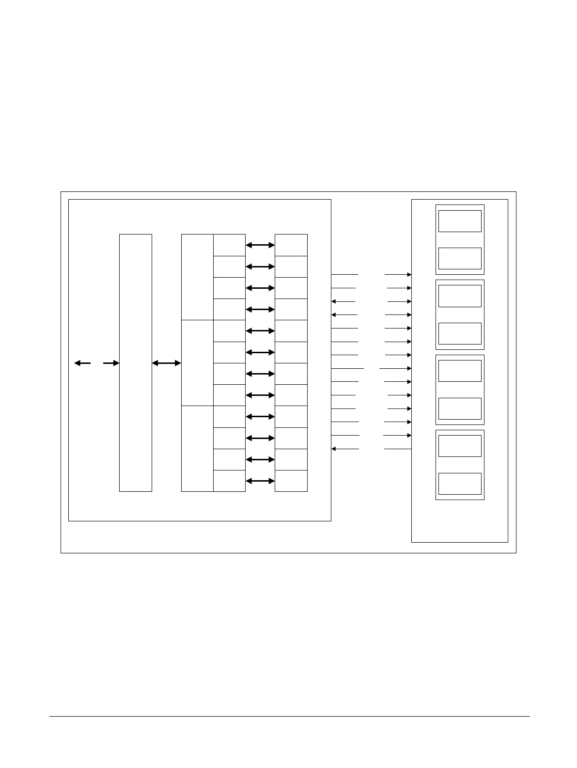
2.14 FPGA DDR4 memory interface
The MPS3 board provides 4GB of DDR4 SODIMM and a DDR4 interface to the FPGA.
The DDR4 controller and PHY interface uses the Xilinx Memory Interface Generator (MIG). The
interface is 64‑bit and uses 10 byte lanes.
The interface supports up to 900MHz, 1800MT/s, with the supplied SODIMM
(MTA4ATF51264HZ-2GB31).
The following figure shows the FPGA DDR4 memory interface.
MPS3 FPGA Prototyping Board
Kintex XCKU115 FPGA
Byte
Lane 1
CK[1:0]
AXI
Byte
Lane 2
Byte
Lane 3
Byte
Lane 4
Byte
Lane 5
Byte
Lane 6
Byte
Lane 7
Byte
Lane 8
Byte
Lane 9
Byte
Lane 10
Byte
Lane 11
Byte
Lane 12
I/O
I/O
I/O
I/O
I/O
I/O
I/O
I/O
I/O
I/O
I/O
I/O
I/O
bank 1
I/O
bank 2
I/O
bank 3
MIG
DQ[63:0]
DQS[7:0]
DM[7:0]
CS[1:0]
BA[1:0]
BG[1:0]
ACT
A[16:0]
CKE[1:0]
ODT[1:0]
RESET
PARIN
ALERT
4GB DDR4
SODIMM
MTA4ATF51264HZ-2G3B1
512MB
Group 0
512MB
Group 1
Bank 1
512MB
Group 0
512MB
Group 1
Bank 2
512MB
Group 0
512MB
Group 1
Bank 3
512MB
Group 0
512MB
Group 1
Bank 4
Figure 2-18 Kintex XCKU115 FPGA DDR4 memory interface
2 Hardware description
2.14 FPGA DDR4 memory interface
100765_0000_04_en Copyright © 2017–2020 Arm Limited or its affiliates. All rights
reserved.
2-41
Non-Confidential
 Loading...
