A.1 Debug connectors
The MPS3 board provides connectors that support P-JTAG processor debug, F-JTAG FPGA debug,
16‑bit and 4‑bit trace, and SWD.
This section contains the following subsections:
• A.1.1 20-pin IDC connector on page Appx-A-71.
• A.1.2 10-pin IDC connector on page Appx-A-72.
• A.1.3 20-pin Cortex debug and ETM connector on page Appx-A-72.
• A.1.4 38-pin MICTOR connector on page Appx-A-73.
• A.1.5 14-pin F-JTAG ILA connector on page Appx-A-74.
• A.1.6 Debug USB 2.0 connector on page Appx-A-75.
A.1.1 20-pin IDC connector
The MPS3 board provides one 1V8 20‑pin IDC connector that supports P‑JTAG processor debug to
enable connection of DSTREAM, or a compatible third‑party debugger. The connector also supports
Serial Wire Debug (SWD).
The 20‑pin IDC connector connects to general‑purpose pins on the FPGA. The availability of P‑JTAG or
SWD depends on the design that you implement in the FPGA.
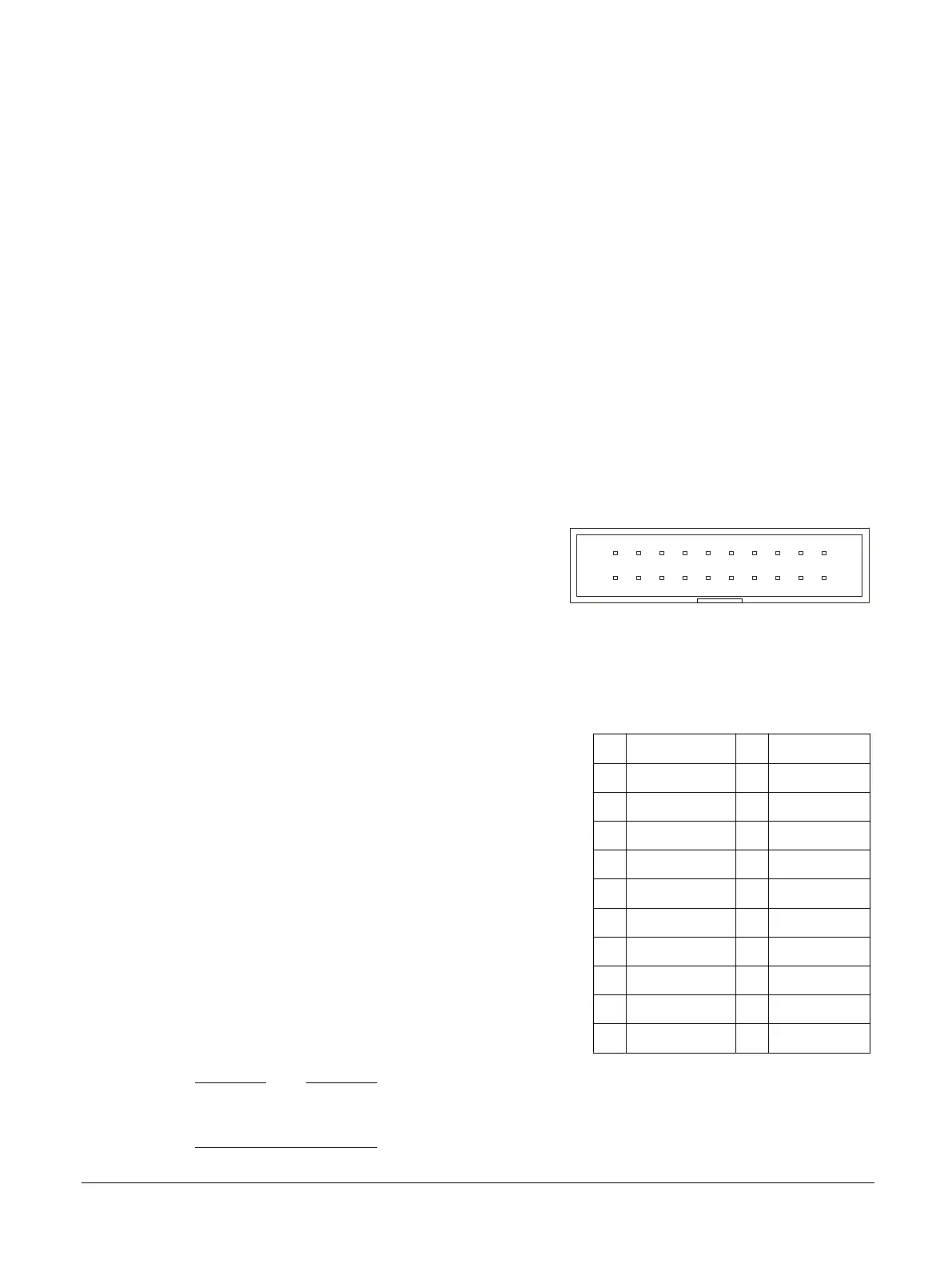
The following figure shows the 20‑pin IDC connector, J14.
1 19
2 20
Figure A-1 20-pin IDC connector
The following table shows the pin mapping for each P‑JTAG and SWD signal on the 20‑pin IDC
connector.
Table A-1 20-pin IDC connector, J14, pin mapping
Pin Signal Pin Signal
1 1V8_REF 2 1V8
3 nTRST 4 GND
5 TDI 6 GND
7 SWDIO/TMS 8 GND
9 SWDCLK/TCK 10 GND
11 GND/RTCK 12 GND
13 SWO/TDO 14 GND
15 nSRST 16 GND
17 NC/DBGRQ 18 GNDDETECT
19 NC/DBACK 20 GND
Note
• Pins 1, 3, 5, 7, 13, 15, and 19 have pullup resistors to 1V8.
• Pins 9, 11, and 17 have pulldown resistors to GND.
A Signal descriptions
A.1 Debug connectors
100765_0000_04_en Copyright © 2017–2020 Arm Limited or its affiliates. All rights
reserved.
Appx-A-71
Non-Confidential
 Loading...
