II-11
2.3 MAIN PCB
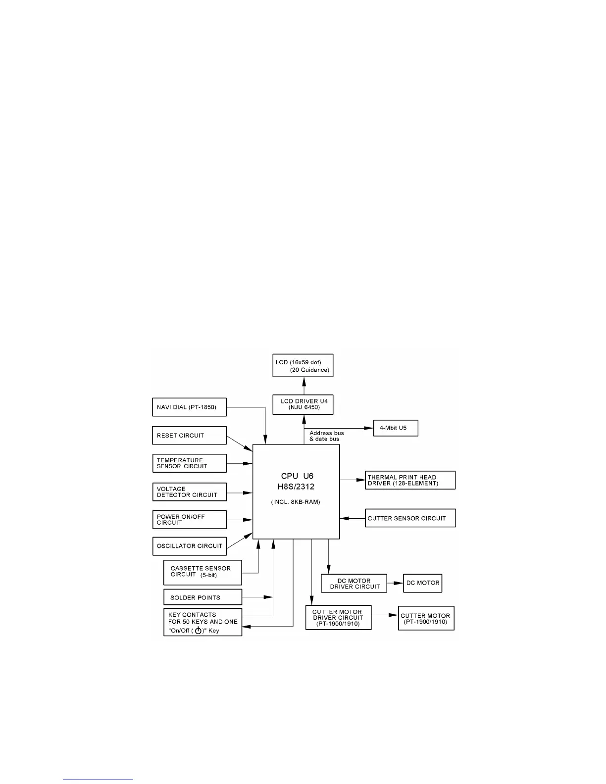
2.3.1 Block Diagram
Fig. 2.3-1 shows a block diagram of the main PCB. The main PCB consists of the following:
(1) CPU
(2) ROM (Masked)
(3) Key contacts matrix and solder points
(4) Power ON/OFF circuit and power saving circuit
(5) DC motor driver circuit
(6) Cutter motor driver circuit (PT-1900/1910)
(7) Thermal head drive circuit
(8) Voltage detector circuit and temperature sensor circuit
(9) Cassette sensor circuit
(10) Cutter sensor circuit
(11) Oscillator circuit
(12) Reset circuit
(13) LCD driver circuit
(14) Navi dial (PT-1850)
Fig. 2.3-1 Block Diagram of Main PCB
 Loading...