190
H27U1G8F2BTR-BCPinFunction
H27U1G8F2BTR-BCBlockDiagram
Rev 1.1 / Sep. 2009 6
1
H27U1G8F2B Series
1 Gbit (128 M x 8 bit) NAND Flash
1.2 PIN DESCRIPTION
Table 2 : Pin Description
NOTE :
1. A 0.1uF capacitor should be connected between the Vcc Supply Voltage pin and the Vss Ground pin to decouple the
current surges from the power supply. The PCB track widths must be sufficient to carry the currents required during
program and erase operations.
Pin Name Description
IO0 ~ IO7
DATA INPUTS/OUTPUTS
The IO pins allow to input command, address and data and to output data during read / program
operations. The inputs are latched on the rising edge of Write Enable (WE
). The I/O buffer float to
High-Z when the device is deselected or the outputs are disabled.
CLE
COMMAND LATCH ENABLE
This input activates the latching of the IO inputs inside the Command Register on the Rising edge of
Write Enable (WE
).
ALE
ADDRESS LATCH ENABLE
This input activates the latching of the IO inputs inside the Address Register on the Rising edge of
Write Enable (WE
).
CE
CHIP ENABLE
This input controls the selection of the device.
WE
WRITE ENABLE
This input acts as clock to latch Command, Address and Data. The IO inputs are latched on the rise
edge of WE
.
RE
READ ENABLE
The RE
input is the serial data-out control, and when active drives the data onto the I/O bus. Data is
valid tREA after the falling edge of RE which also increments the internal column address counter by
one.
WP
WRITE PROTECT
The WP
pin, when Low, provides an Hardware protection against undesired modify (program / erase)
operations.
R/B
READY BUSY
The Ready/Busy output is an Open Drain pin that signals the state of the memory.
Vcc
SUPPLY VOLTAGE
The Vcc supplies the power for all the operations (Read, Write, Erase).
Vss GROUND
NC NO CONNECTION
Rev 1.1 / Sep. 2009 15
1
H27U1G8F2B Series
1 Gbit (128 M x 8 bit) NAND Flash
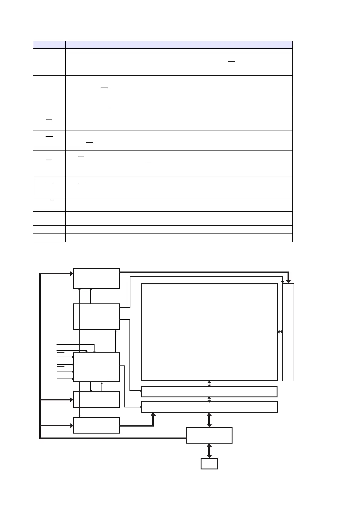
Figure 4 : Block Diagram
ADDRESS
REGISTER/
COUNTER
PROGRAM
ERASE
CONTROLLER
HV GENERATION
COMMAND
INTERFACE
LOGIC
COMMAND
REGISTER
DATA
REGISTER
IO
RE
BUFFERS
Y DECODER
PAGE BUFFER
X
D
E
C
O
D
E
R
1024 Mbit + 32 Mbit
NAND Flash
MEMORY ARRAY
WP
CE
WE
CLE
ALE
A27 ~ A0
 Loading...