(
(
C'
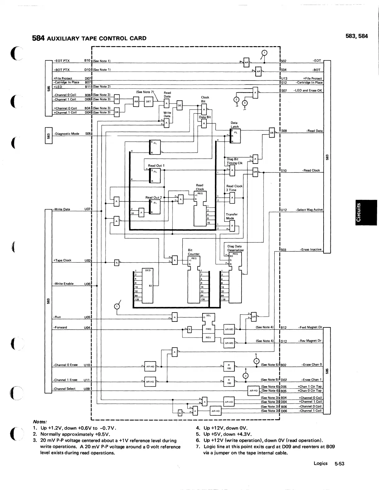
584
AUXILIARY
TAPE CONTROL CARD
....
AA
r----------------------------------------,
o I
11
IS02
I
~
-EOTPTX
1
Bl0
i(See
Note
1)
-EOT
~
~AAP_-----r!ls=~~--------~-B~O~T~
IU13
!
~BOT
PTX
DIO
1
(See
Note
1)
!
+File Protect
-Catridge
In
Place
II!
+LED
II>
-Channel 0
Coil
-Channel
1
Coil
+Channel
0 Coil
+Channel
1
Coil
~
~
-Diagnostic Mode
r--
-Write
Data
D071
B07
BIll
(See
Note
2)
!
B061
(See
Note
3)
D061
(See
Note
3)
OR
I
(See
Not.
7)
..-.
AA
DET
B~
I
(See
Note
3)
D~
(See
Note
3)
OR
I
I
Read
Date
A
Write
Date
A
DE
Data
Latch
I
505
-qB
I-----flD:te
A
: Bit
1
2,
r--------------------------------"
~
FL
------------------------------+-~--~----~~R
_.
!
U07
!
~U~
[
0;;:-
L
t'=---------IA
P_--------------'
I
Diag
Bit
~ngClk
,~tl
.~I.I
~l'~SFL~------~~~~r-Hro
R
Read
Bit
Deserializer
AEG
so
~
iagDate
G
R
~t§1
counter,
~!
REG
/-+:..:T"'ap"'e::..;c"'IOC=k
____
--"U"'
02
'l'jf--H
.....
__
-l
N
1>---------------1----"'\
A
:'
L....
1..-
""-
1
..!..-
-;;co
.!--
I -'--
L-
L-
L-
llL-
iE-
1
.L..
.L-
U061
c!--
a,
'-
L-
,
•
!
.lL
-"'--
I
.1L
.ilL-
-Write
Enable
~
P"-_
I
sf
~
;;.
1
-=---
L.....---=--
1
t::I
II>
-Run
1512
I
1
I
I
I
I
1
1509
I
I
1
I
1
1
1
1
510
I
1
I
I
1
1
I
IU12
I
I
I
I
I
I
I
1503
+File Protect
-Cartridge
I n
Place
-LED
and
Erase
OK
-Read
Data
-Read
Clock
-Select
Mag
Active
-Erase
Inactive
~
F"-"--
___
-"U"'05,I--+-+-
__________
...l:>f
A
I-----;G
SEL
f?Et:A
I
I-'-=:::.::'--
____
-"'U~"'I'+-
i++-
______________________________
-.-''''I
N
FWD
AR.MD
(See
Note
4)
B12
-Forward
-Fwd
Magnet
Dr
r--
I I
1
REV
I
I
(See
Note
4)
1
D12
-Rev
Magnet
Dr
I
AR·MO
P---+----....:==='--'-1HIP'-'
......
----==="-=-'-t
I
~
I
p=====--_u"-I'-'o,Ic-H
______________
___''''I
AR.HD
1 I
~
" R
~
(See
Not.
5102
I
180,l
I
Ulll
R
~
(See
Note S)I
D02
p=="'-"='-~'-'-Ic-H-----------------''''I
AR·HD
f>---
......
----------------------''''I
uool
180
(See
Note
6)1
D05
p:====---,-"'''''-il'-H--------------------------------------------------------~
AA·HD
h(See
Note
6)1
B05
I
(See
Note
3)
I
B~
-Channel
0
erase
-Channel 1
Erase
-Channel
Select
'--
-Erase
Chan
0
~
-Erase
Chan
1
+Chan 1
Ctr
Tap
+Chan
0 Ctr Tap
+Channel
0 Coil
1 " A
AA·HO
1--________
..J(i2see!!!W:N!!!0~te'_'3!Lj) !-,D!!.~!:!....
____
,!<!!=~-"""
+Channel
1
Coil
-Channel 0
Coil
I
~
(seeNote31IB06
1
N A
AA·HO
1-
______________
(::See:::::..:N.::o
oo
te::.:3"'Ij-'D"'0"'6'--
__
----'==..:...:=-L...J
I I
-Channel 1 Coil
~
Notes:
L
________________
~~-------------_------~
1.
Up
+1.2V,
down
+0.6Vto
-0.7V.
2. Normally approximately +9.5V.
3.
20
mV
poP
voltage centered
about
a
+1
V reference level during
write operations. A
20
mV
poP
voltage
around
a 0 volt reference
level
exists during read operations.
4.
Up +12V,
down
OV.
5.
Up +5V, down +4.3V.
6.
Up
+12V (write operation),
down
OV
(read operation).
7.
Logic line
at
this
point exits card
at
D09
and
reenters
at
BOO
via
a jumper
on
the
tape
internal cable.
Logics 5-53
583,584
 Loading...