Troubleshooting 4-7
Power supply
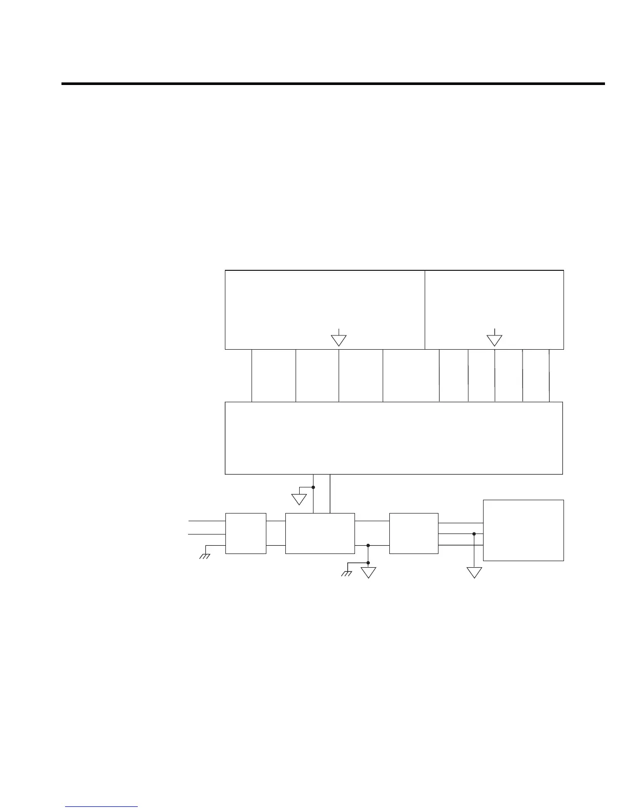
Figure 4-3 shows a block diagram of the Model 2430 power delivery system.
The offline switching power supply provides all power for the instrument while providing
universal inputs and power factor correction for the 120/240V line. The digital board runs off of
5V and 12V supplies derived from the switcher. The +12VD supply is set to program the flash
ROM. (See Digital circuitry below.)
A constant-frequency switching supply runs off the +24VD supplies and generates all the float-
ing and output supply voltages for the analog board: +5V and ±15V, ±42V and ±150V.
Analog Board
+15V +5V
F
-15V
FF F
Output Stage
-150V -42V +42V +150V
O
Constant Frequency
Low Noise Floating
Switching Supply
+24Vdc
D
Line
Neutral
+5Vdc
D
+12Vdc
PFC
DC/DC
Converter
D
Digital
Circuits
+24dc
DC
Regulators
Figure 4-3
Power supply block
diagram
Output stage
Figure 4-4 shows a simplified schematic of the output stage.
The Model 2430 output stage serves two purposes: (1) it converts signals from floating com-
mon to output common, and (2) it provides both voltage and current amplification. The output
stage drive transistors are biased in class B configuration to prevent the possibility of thermal
runaway with high-current output values.
Output transistors Q518 and Q521 are cascoded with output MOSFETs Q516 and Q523. All
other MOSFETs and transistors are slaves, and the voltages across these devices are determined
 Loading...