A/D
Control/Data
Voltage Source
Control
ROM
U15, U16
RAM
U12, U14
Reset
E PROM
U17
2
A/D Interface
U9, U25
Microprocessor
U3
Serial
Interface
U4
GPIB
U6, U13
U20
RS-232 Interface
IEEE-488 Interface
To Display
Board Controller
Trigger
U23
Digital I/O
U7
Trigger
Digital
I/O
16.78MHz
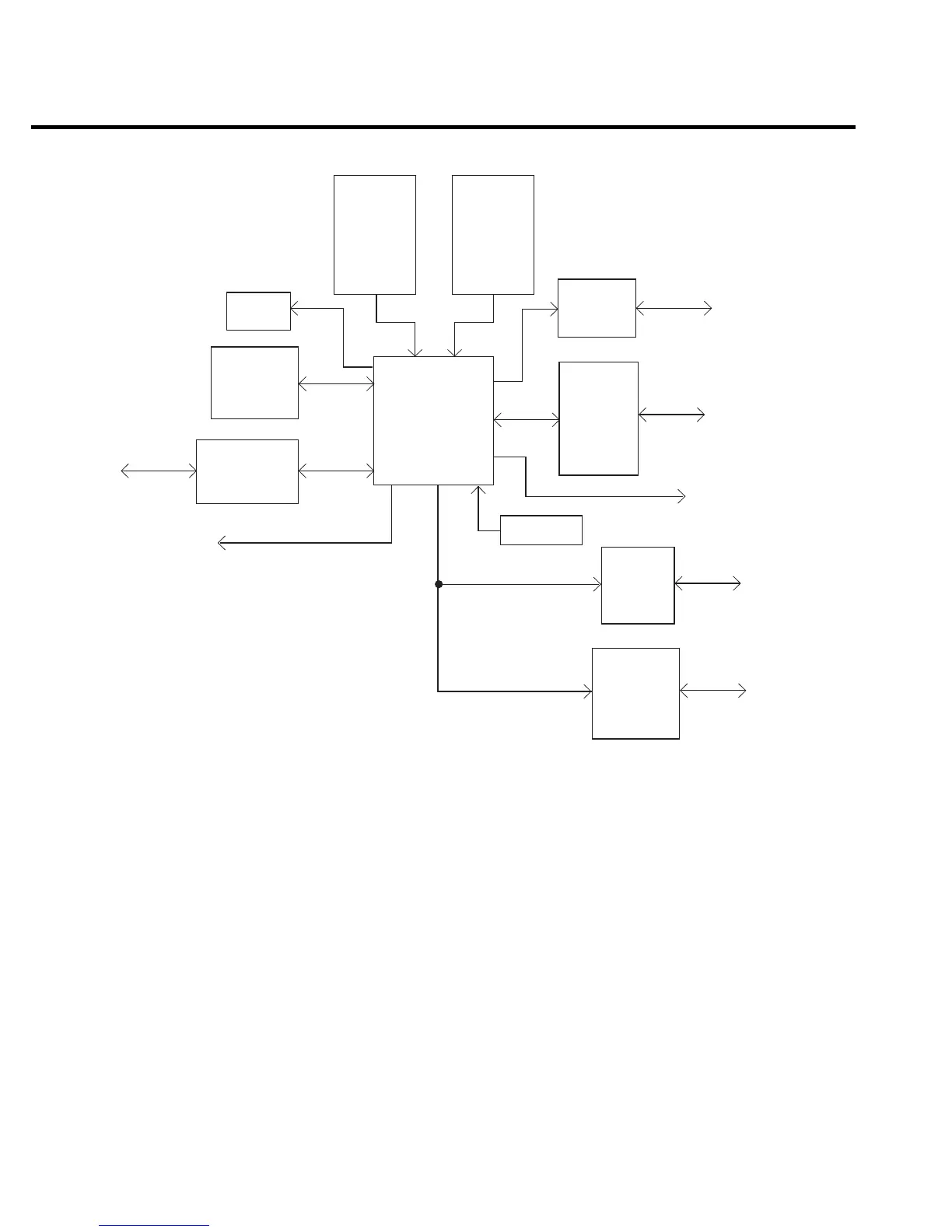
Figure 4-5
Digital circuitry
block diagram
4-10 Troubleshooting
Display board circuit theory
Display board components are shown in the digital circuitry block diagram in Figure 4-5.
U902 is the display microcontroller that controls the VFD (vacuum fluorescent display) and
interprets key data. The microcontroller has four peripheral I/O ports that are used for the vari
-
ous control and read functions.
Display data is serially transmitted to the microcontroller from the digital board via the TXB
line to the microcontroller PD0 terminal. In a similar manner, key data is serially sent back to
the digital board through the RXB line via PD1. The 4MHz clock for the microcontroller is gen
-
erated on the digital board.
DS901 is the VFD (vacuum fluorescent display) module, which can display up to 49 charac-
ters. Each character is organized as a 5 × 7 matrix of dots or pixels and includes a long under-
bar segment to act as a cursor.
 Loading...