NVIDIA Jetson TX2 NX DG-10141-001_v1.1 | 11
Chapter 5. Power
Power for the module is supplied on the VDD_IN pins and is nominally 5.0V (see the
Jetson TX2
NX Data Sheet
for supply tolerance and maximum current).
CAUTION: Jetson TX2 NX is not hot-pluggable. When installing the module, the main power
supply should not be connected. Before removing the module, the main power supply (to VDD_IN
pins) must be disconnected and allowed to discharge below 0.6V.
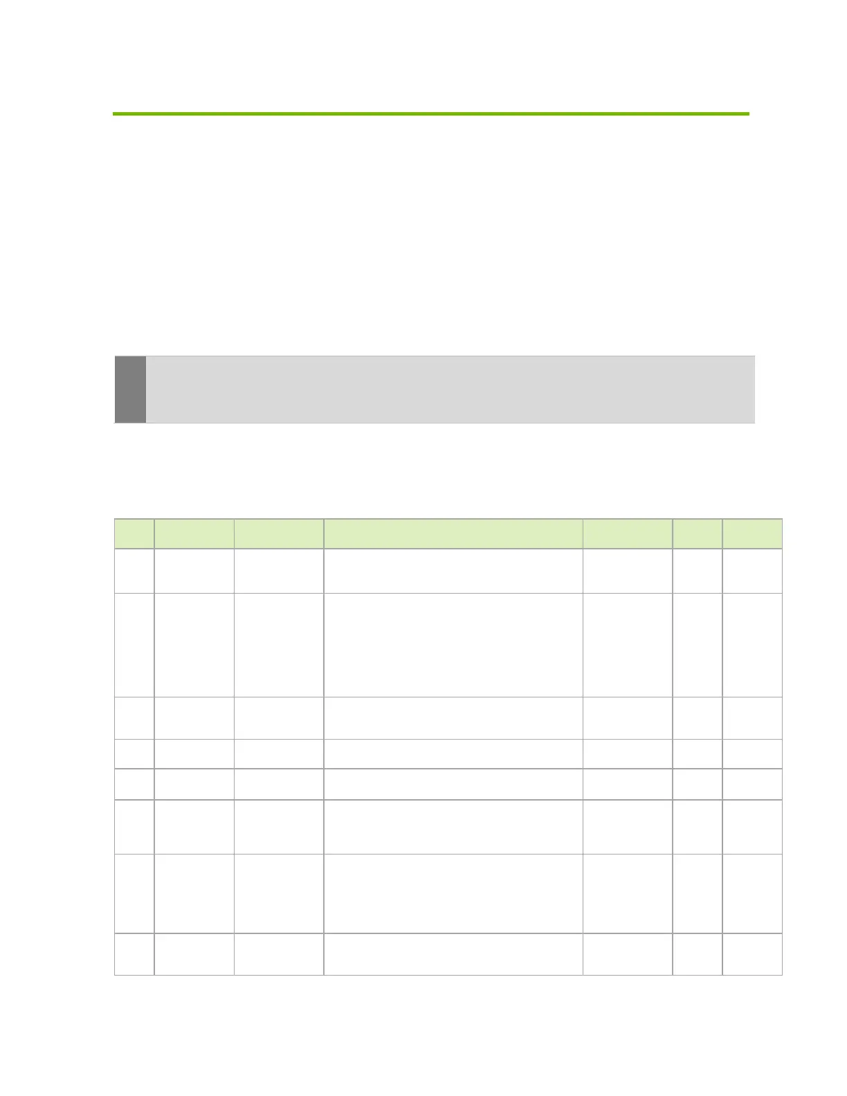
Table 5-1. Jetson TX2 NX Power and System Pin Descriptions
Pin # Module Pin
Name
Tegra X2 Signal Usage/Description Usage on DevKit
Carrier Board
Direction Pin Type
251
↓
260
VDD_IN − Main power – Supplies PMIC and other regulators Main DC input Input 5.0V
235
PMIC_BBAT −
PMIC Battery Back-up. Optionally used to provide back-up
power for the Real-Time-Clock (RTC). Connects to
Lithium Cell or super capacitor on Carrier Board. PMIC is
source when charging cap or coin cell. Super cap or coin
cell is source when system is disconnected from power.
Charging is enabled by default in software. If non-
rechargeable battery is to be used, charging should be
disabled.
Battery Back-up
using Super-
capacitor
Bidir
Input
Range:
1.65V-5.5V
Output
Options:
2.5V, 3.0V,
3.3V, 3.5V
RECOVERY*
Force Recovery strap pin. Held low when SYS_RESET*
goes high (i.e. during power-on) places system in USB
recovery mode.
1.8V
SLEEP/WAKE* BUTTON_PWR_ON Sleep/Wake. Configured as GPIO for optional use to
indicate the system should enter or exit sleep mode.
Automation header Input CMOS –
5.0V
233
SHUTDOWN_
REQ*
− Used by the module to request the carrier board to shut
down. ~5kΩ pull-up to VDD_IN (5V) on the module.
System Output Open Drain,
5.0V
POWER_EN (PMIC EN0
through converter
logic)
Signal for module on/off: high level on, low level off.
Connects to module PMIC EN0 through converter logic.
POWER_EN is routed to a Schmitt trigger buffer on the
module. 100kΩ pulldown on the module.
System Input Analog 5.0V
239 SYS_RESET* SYS_RESET_IN_N Module Reset. Reset to the module when driven low by the
carrier board. Used as carrier board supply enable when
driven high by the module when module power sequence
is complete. Used to ensure proper power on/off
sequencing for between module and carrier board
supplies. 10kΩ pull-up to 1.8V on the module.
Automation header Bidir Open Drain,
1.8V
178 MOD_SLEEP* GPIO_PA6 Module Sleep. When active (low), indicates module has
gone to Sleep (SC7) mode. This pin is controlled by system
software and should not be modified.
HDMI termination
pull-down FET
control disable
Output CMOS –
1.8V

 Loading...


