Miscellaneous Interfaces
NVIDIA Jetson TX2 NX DG-10141-001_v1.1 | 61
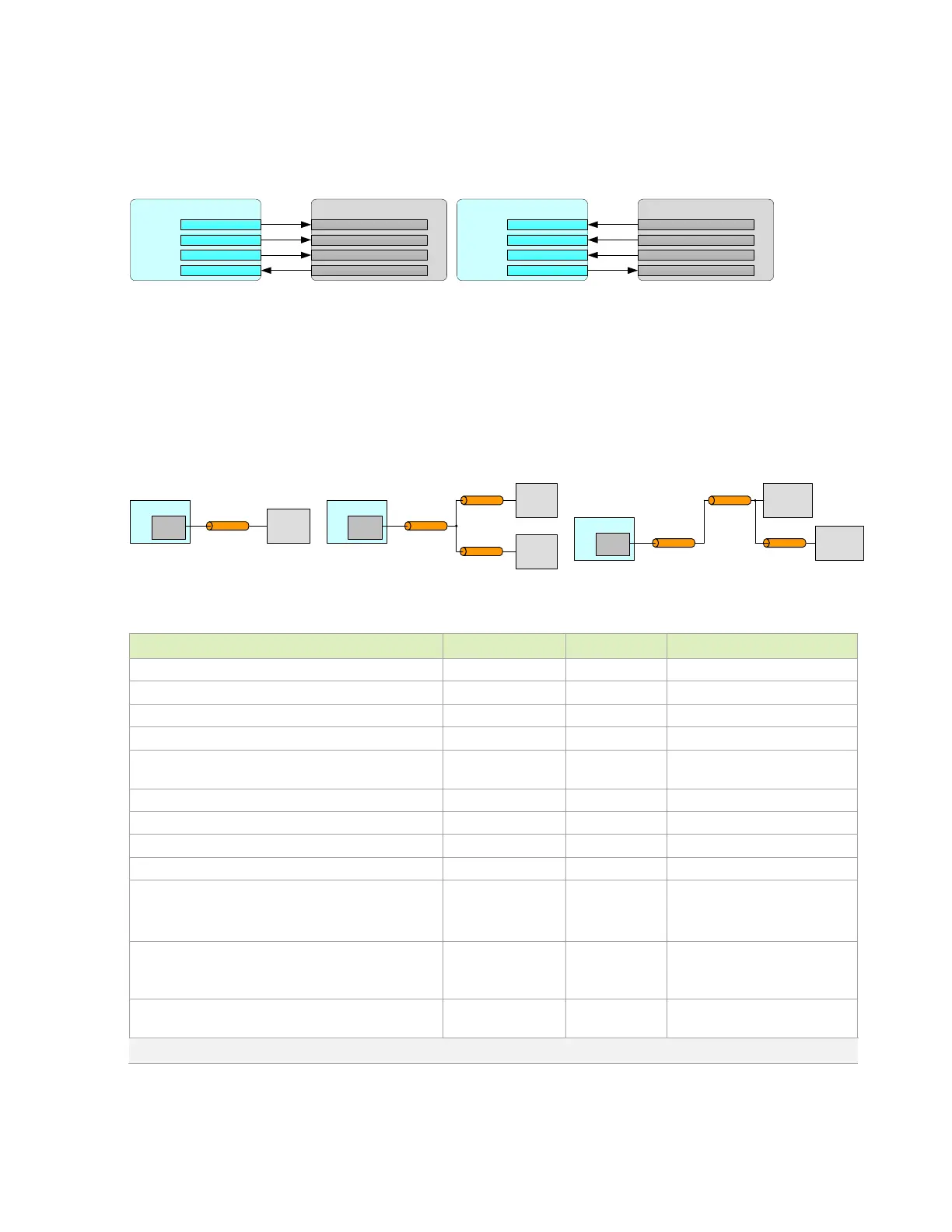
Figure 11-3 shows the basic connections used.
Figure 11-3. Basic SPI Master and Slave Connections
Jetson Master
SPIn_CSx
SP In_SCK
SP In_MO SI
SP In_MISO
SPI Slave Device
CS (Chip Select)
CLK ( Clock)
MOSI (Ma ster out, Sla ve i n)
MISO (Master in, Sla ve out)
Jetson Slave
SPIn_CSx
SP In_SCK
SP In_MO SI
SP In_MISO
SPI Master Device
CS (Chip Select)
CLK ( Clock)
MOSI (Ma ster out, Sla ve i n)
MISO (Master in, Sla ve out)
11.2.1 SPI Design Guidelines
Figure 11-4 shows the SPI topologies and Table 11-5 gives the SPI interface signal routing
requirements.
Figure 11-4. SPI Topologies
Jetson
SPI
Device
#1
Main trunk
SPI
Device
#2
SPI
Device
#1
Main trunk
SPI
Device
#2
Branch-A
Branch-B
Branch-A
Branch-B
2x-Load Star Topology 2x-Load Daisy Topology
SPI
Device
Main trunk
Tegra
Jetson
Tegra
Jetson
Tegra
Point-Point Topology
Table 11-5. SPI Interface Signal Routing Requirements
Parameter Requirement Units Notes
Max frequency 65 MHz
Configuration / device organization 4 load
Max loading (total of all loads) 15 pF
Reference plane GND
Breakout region impedance
Minimum width
and spacing
Max PCB breakout delay 75 ps
Trace impedance 50 – 60 Ω ±15%
Via proximity (signal to reference) < 3.8 (24) mm (ps) See note
Trace spacing (Microstrip / Stripline) 4x / 3x dielectric
Max trace length/delay (PCB main trunk) for
and
2x-load star/daisy
Point-point
195 (1228)
120 (756)
mm (ps)
Max trace length/delay (Branch-A) for
and
2x-load star/daisy
75 (472) mm (ps)
Max trace length/delay skew from
and
to
16 (100) mm (ps) At any point
Note: Up to four signal vias can share a single GND return via.

 Loading...


