USB and PCI Express
NVIDIA Jetson TX2 NX DG-10141-001_v1.1 | 25
6.2.1 PCIe Design Guidelines
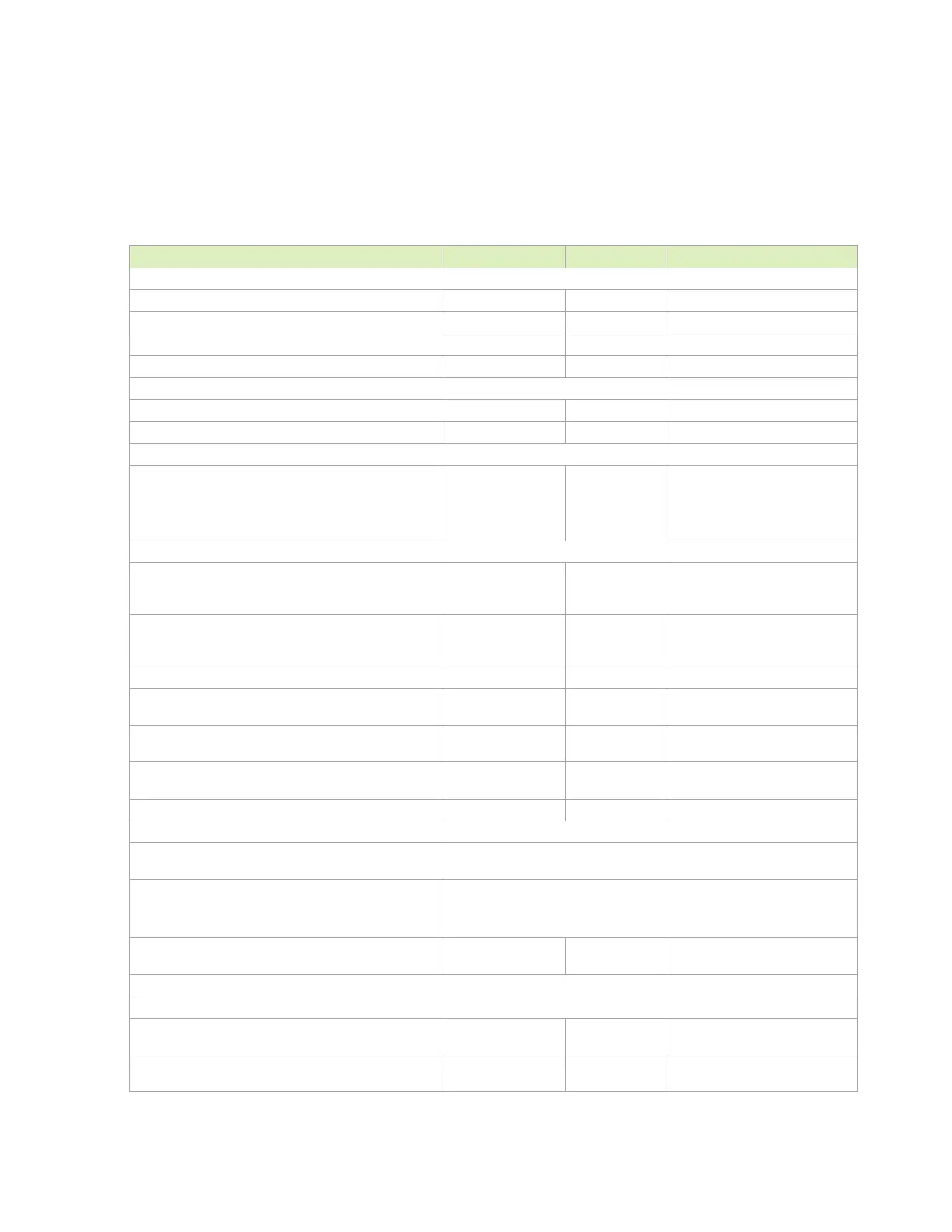
Table 6-9 and Figure 6-8 provide the signal routing requirements for the PCIe interface.
Table 6-9. PCIe Interface Signal Routing Requirements
Parameter Requirement Units Notes
Specification
Data rate / UI period 5.0 / 200 Gbps / ps 2.5GHz, half-rate architecture
Configuration / device organization 1 Load
Topology Point-point Unidirectional, differential
Termination 50 Ω To
Single Ended for P and N
Impedance
Trace Impedance (diff / SE) 85 / 50 Ω ±15%. See Note 1
Reference plane
Spacing
Trace Spacing (Stripline/Microstrip)
pair – pair
To plane and capacitor pad
To unrelated high-speed signals
3x / 4x
3x / 4x
3x / 4x
Dielectric
See Note 2
Length/Skew
Trace loss characteristic @ 2.5 GHz < 0.7 dB/in The following max length is
derived based on this
characteristic. See Note 3
Breakout region (max length) 41.9 ps Minimum width and spacing. 4x
or wider dielectric height spacing
is preferred
Max trace length/delay 5.5 (880) in (ps)
Max PCB via distance from the BGA 41.9 ps Max distance from BGA ball to
first PCB via.
PCB within pair (intra-pair) skew 0.15 (0.5) mm (ps) Do trace length matching before
hitting discontinuities
Within pair (intra-pair) matching between subsequent
discontinuities
0.15 (0.5) mm (ps)
Differential pair uncoupled length 41.9 ps
Via
Via placement Place
vias as symmetrically as possible to data pair vias.
via
distance should be placed less than 1x the diff pair via pitch
Max # of vias
PTH vias
Micro-vias
2 for TX traces and 2 for RX trace
No requirement
Max via stub length 0.4
mm
Longer via stubs would require
review
Routing signals over antipads Not allowed
AC Cap
Value (Min/Max) 0.075 / 0.2
uF
Only required for TX when routed
to connector
Location (max length to adjacent discontinuity) 8
mm
Discontinuity such as edge finger,
component pad

 Loading...


