Power
NVIDIA Jetson TX2 NX DG-10141-001_v1.1 | 12
Pin # Module Pin
Name
Tegra X2 Signal Usage/Description Usage on DevKit
Carrier Board
Direction Pin Type
210 CLK_32K_OUT − Sleep/Suspend clock M.2 Key E Output
CMOS –
1.8V
Notes:
1. In the Type/Dir column, Output is from Jetson TX2 NX. Input is to Jetson TX2 NX. Bidir is for Bidirectional signals.
2. The directions for FORCE_RECOVERY* and SLEEP/WAKE* signals are true when used for those functions. Otherwise as GPIOs,
the direction is bidirectional.
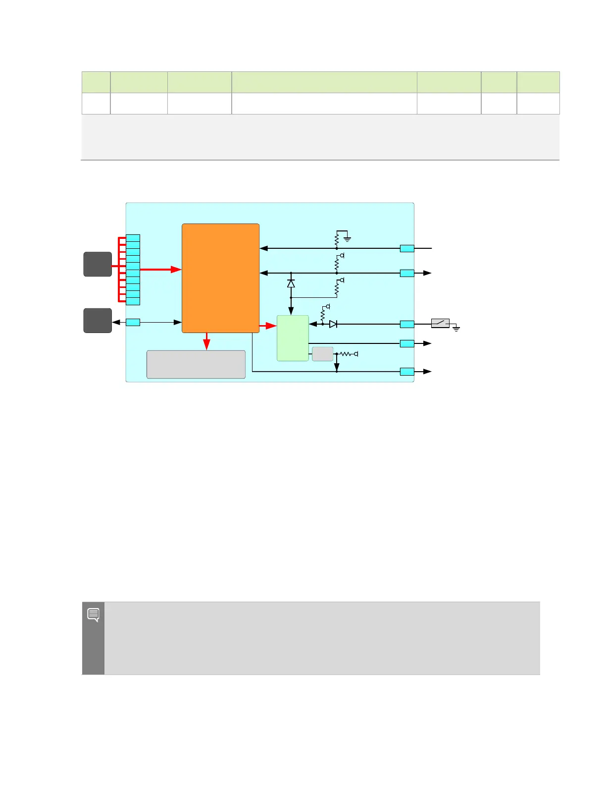
Figure 5-1. Jetson TX2 NX Power and Control Block Diagram
Jetson
Main 5V
Power
Source
255
256
257
258
259
260
235
Memory/Peripherals
LPDDR4, eMMC,
Ethernet
Power Subsystem
Tegra X2
PMIC_BBAT
VDD_IN
233
240
239
237
POWER_EN
SYS_RESET*
SLEEP/WAKE*
MOD_SLEEP *
SHUTDOWN_REQ*
To Carrier Board – Used to force
power off if shutdown request
(T he rm al S hut down, P owe r Bad or
Software Shutdown, etc.) is received
From Carrier Board power
ON/ OF F c ontrol logic
System Reset from Carrier
Board. Carrier Board power
enable f rom Module.
Optional Sleep/Wake Button
SLE EP/WAKE
Super
Cap or
Li Cell
251
252
253
254
178
Indicates Module is entering
Sleep (SC7) mode
10 0kΩ10 kΩ
VDD_1V8
4. 7kΩ
VDD_1V8
10 0kΩ
VDD_1V8
Lev el
Shifter
~5kΩ
VDD_IN (5V)
5.1 Power Supply and Sequencing
This section details the power supply and sequencing for the Jetson TX2 NX module.
5.1.1 Power Handshake Signals
The carrier board receives the main power source and uses this to generate the enable to
Jetson TX2 NX (
POWER_EN) after the carrier board has ensured the main supply is stable and
the associated decoupling capacitors have charged. The carrier board supplies are not
enabled at this time. Once
POWER_EN is driven active (high), the module begins to Power-ON.
When the module Power-ON sequence has completed, the
SYS_RESET* signal is released
(pulled high on module) and this is used by the carrier board to enable its various supplies.
Note: The carrier board cannot drive high or pull high any signals that are associated with the
module when the module rails are off. If the designer cannot guarantee a signal will not be
driven or pulled high, then either the power rail related to that signal should be left off, or the
signals would need to be buffered to isolate them from the module pins. The buffers should only
be enabled towards the module when SYS_RESET* goes high.