Display
NVIDIA Jetson TX2 NX DG-10141-001_v1.1 | 37
The following figures show the eDP and DP interface signal routing requirements.
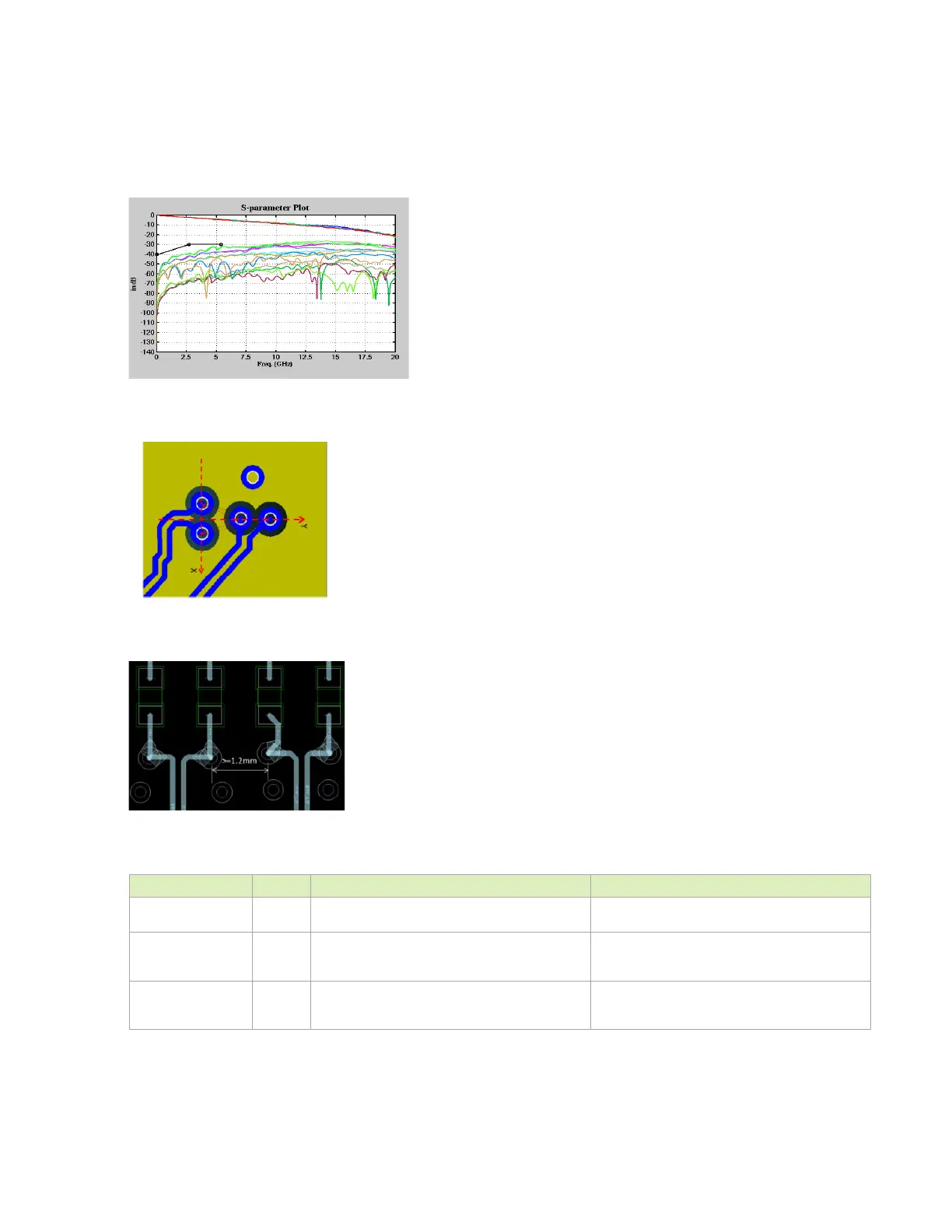
Figure 7-4. S-parameter
Figure 7-5. Via Topology #1
Figure 7-6. Via Topology #2
Table 7-8. eDP and DP Signal Connections
Module Pin Name Type Termination Description
DPx_TXD[3:0]_N/P O Series 0.1uF capacitors and ESD to
on all.
eDP/DP Differential CLK/Data Lanes: Connect to
matching pins on display connector.
DPx_AUX_N/P I/OD
Series 0.1uF capacitors. 100kΩ pulldown on
DP0_AUX_P and 100kΩ pull-up to VDD_3V3_SYS on
DP0_AUX_N. ESD to
on both.
eDP/DP: Auxiliary Channels
: Connect to
-/+
on display connector.
DPx_HPD I
From module pin: 10kΩ pull-up to 1.8V, level shifter
and 100kΩ pulldown on connector side of shifter and
ESD to
.
: Connect to
pin on
display connector through level shifter.

 Loading...


