Display
NVIDIA Jetson TX2 NX DG-10141-001_v1.1 | 36
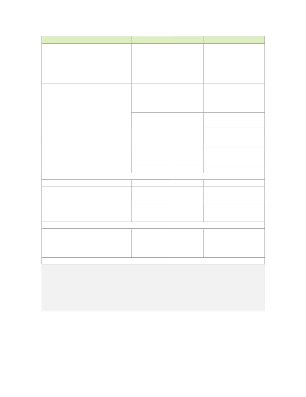
Parameter Requirement Units Notes
Impedance dip
Recommended via dimension for impedance control
Drill/Pad
Antipad
Via pitch
≥97
≥92
200/400
>840
≥880
Ω @ 200ps
Ω @ 35ps
um
um
um
The via dimension is required for
HDMI-DP co-layout.
Topology Y-pattern is recommended
keep symmetry
Y-pattern helps with Xtalk
suppression. It can also reduce the
limit of pair-pair distance. Need
review (NEXT/FEXT check) if via
placement is not Y-pattern. See
Figure 7-5
For in-line via, the distance from a via of
one lane to the adjacent via from another
lane >= 1.2 mm center-center.
See Figure 7-6
via
Place
via as symmetrically as
possible to data pair vias. Up to four signal
vias (2 diff pairs) can share a single
return via
via is used to maintain a
return path, while its Xtalk
suppression is limited.
Max # of vias
PTH vias
Micro vias
2 if all vias are PTH via
Not limited if total channel loss meets IL
spec
Max via stub length 0.4 mm
AC Cap
Value 0.1 uF Discrete 0402
Max distance from AC cap to connector
No requirement
0.5
in
Voiding
No requirement
Voiding required
: Voiding the plane directly
under the pad 3-4 mils larger than
the pad size is recommended.
Connector
Voiding
No requirement
Voiding required
Standard DP connector:
Voiding requirement is stack-up
dependent. For typical stack-ups,
voiding on the layer under the
connector pad is required to be 5.7
mil larger than the connector pad.
General: See Chapter 15 for guidelines related to Serpentine routing, routing over voids and noise coupling
Notes:
1. For eDP/DP, the spec puts a higher priority on the trace loss characteristic than on the impedance. However, before selecting 85Ω for
impedance, it is important to make sure the selected stack-up, material and trace dimension can achieve the needed low loss
characteristic.
2. Longer trace lengths may be possible if the total trace loss is equal to or better than the target. If the loss is greater, the max trace
lengths will need to be reduced.
3. Do not perform length matching within breakout region. Recommend doing trace length matching to <1ps before vias or any discontinuity
to minimize common mode conversion.
4. The average of the differential signals is used for length matching.

 Loading...


