USB and PCI Express
NVIDIA Jetson TX2 NX DG-10141-001_v1.1 | 20
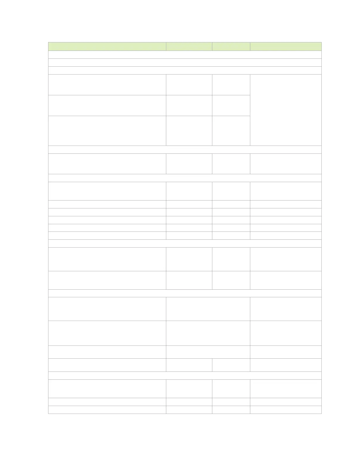
Parameter Requirement Units Notes
The breakout trace width is suggested to be the minimum to increase inter-pair spacing
Do not perform serpentine routing for intra-pair skew compensation in the breakout region
See Figure 6-3
Min inter-SNEXT (between TX/RX)
Breakout
Main-route
4.85x
3x
Dielectric height
This is the recommended
dimension for meeting NEXT
requirement.
Stripline structure in a GSSG
structure is assumed; it holds in
broadside-coupled stripline
structure.
All values are in terms of minimum
dielectric height.
LBRK = Breakout length
Min inter-SFEXT (between TX/TX or RX/RX)
Breakout
Main-route
1x
1x
Inter-pair
spacing
Max length
Breakout
Main-route
11
Max trace length -
LBRK
mm
Trace Spacing
Pair-Pair (inter-pair) (Microstrip / Stripline)
To plane and capacitor pad (Microstrip / Stripline)
To unrelated high-speed signals (Microstrip / Stripline)
4x / 3x
4x / 3x
4x / 3x
dielectric
Trace Length/Skew
Trace loss characteristic @ 2.5GHz < 0.7 dB/in
The following max length is derived
based on this characteristic. See
Note 1.
Breakout region (Max trace delay) 11 mm Minimum width and spacing
Max trace length/delay 152.3 (1014) mm (ps)
Max PCB via distance/delay from pin 6.29 (41.9) mm (ps)
Max within pair (intra-pair) skew 0.15 (1) mm (ps)
Differential pair uncoupled length/delay 6.29 (41.9) mm (ps)
AC Cap
Value 0.1 uF
Smallest size preferred (i.e. 0201).
See note under USB Connection
Diagrams for details on when AC
capacitors are required
Location (max distance to adjacent discontinuities) 8 (53.22) mm (ps)
The AC cap location should be
located as close as possible to
nearby discontinuities
via structure
Y-pattern is strongly recommended (keep
symmetry)
Xtalk suppression is best when
using Y-pattern. Can also reduce
the limit of pair-pair distance. See
Figure 6-4.
GND via
Place
via as symmetrically as
possible to the data pair vias.
Up to 4 signal vias (2 diff pairs) can share a
single
return via"
via is used to maintain return
path, while its Xtalk
suppression is limited.
AC cap pad voiding
GND (or PWR) void under / above the cap is
preferred
Voiding is required if cap size is
0603 or large.
Max via stub length 0.4 mm
long via stub requires review (IL and
resonance dip check).
ESD
Preferred device
Type: Texas Instruments
TPD4I05U06. Optional. Place ESD
component near connector
Max junction capacitance (IO to GND) 0.8 pF
Location (max distance to connector) 8 (53) mm (ps)

 Loading...


