28 Functional Description TB7100 Service Manual
© Tait Electronics Limited October 2005
3.2.3 RF Power Amplifier
RF Power Amplifier
and Switching
The RF PA (power amplifier) is a four-stage line-up with approximately
42dB of power gain. The output of the frequency synthesizer is first buffered
to reduce kick during power ramping. The buffer output goes to a broad-
band exciter IC that produces approximately 200mW output. This is
followed by an LDMOS driver producing up to 2 W output that is power-
controlled. The final stage consists of two parallel LDMOS devices
producing enough power to provide 25W at the RF connector.
Output of RF
Power Amplifier
The output of the RF PA passes through a dual-directional coupler, used for
power control and monitoring. Finally, the output is low-pass-filtered to
bring harmonic levels within specification.
Power Control The steady-state power output of the transmitter is regulated using a
hardware control loop. The forward power output from the RF PA is sensed
by the directional coupler and fed back to the power control loop. The PA
output power is controlled by varying the driver gate bias voltage that has a
calibrated maximum limit to prevent overdrive. The power control signal is
supplied by a 13-bit DAC driven by custom logic.
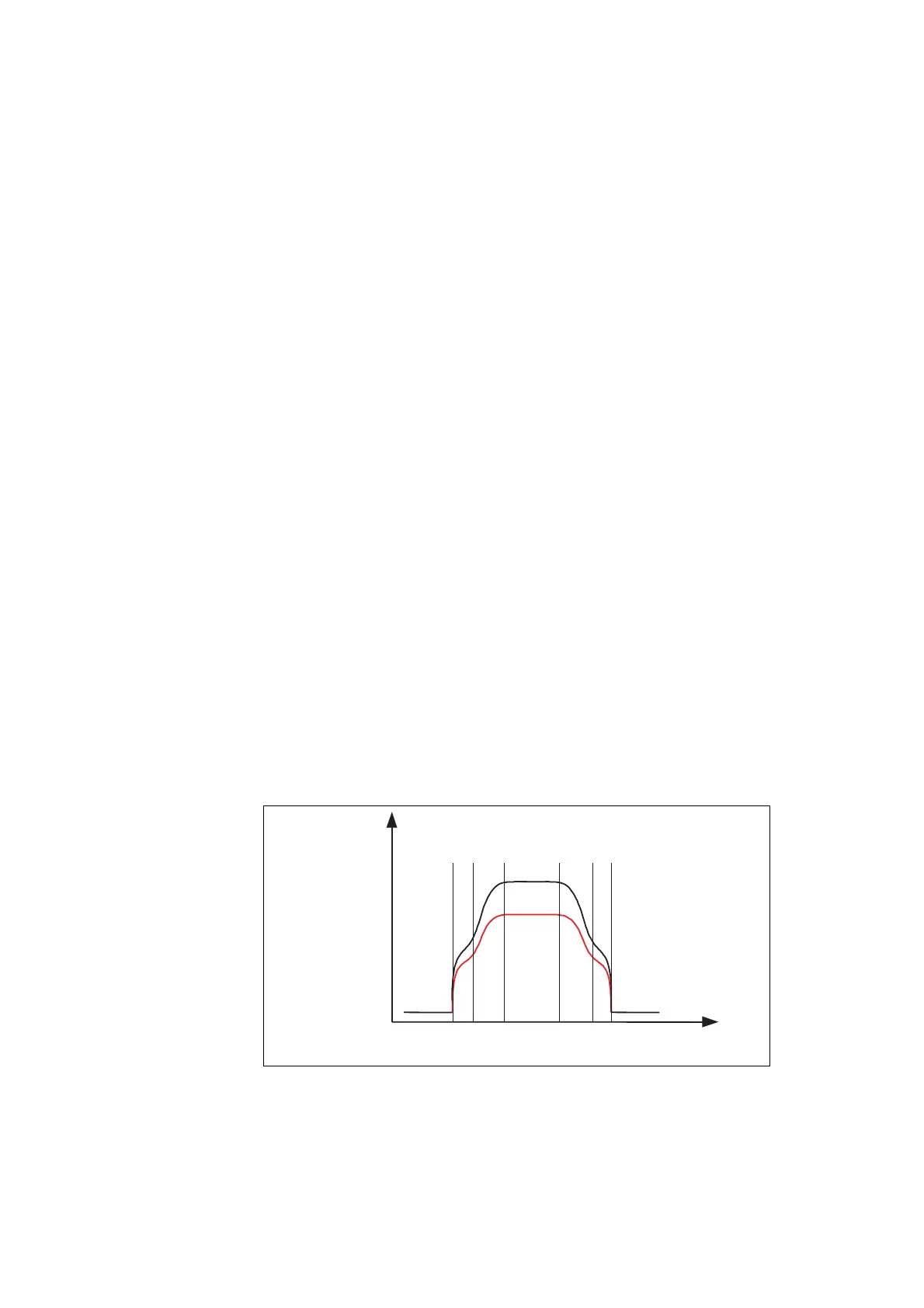
Ramping Power ramp-up consists of two stages:
■ bias
■ power ramping
The timing between these two stages is critical to achieving the correct
overall wave shape in order to meet the specification for transient ACP
(adjacent channel power). A typical ramping waveform is shown in
Figure 3.4.
Figure 3.4 Typical ramping waveforms
Power
ramp
High power
powerLow
Power
Time
Bias
ramp
Bias
ramp
Power
ramp
 Loading...