AC701 Evaluation Board www.xilinx.com 27
UG952 (v1.3) April 7, 2015
Feature Descriptions
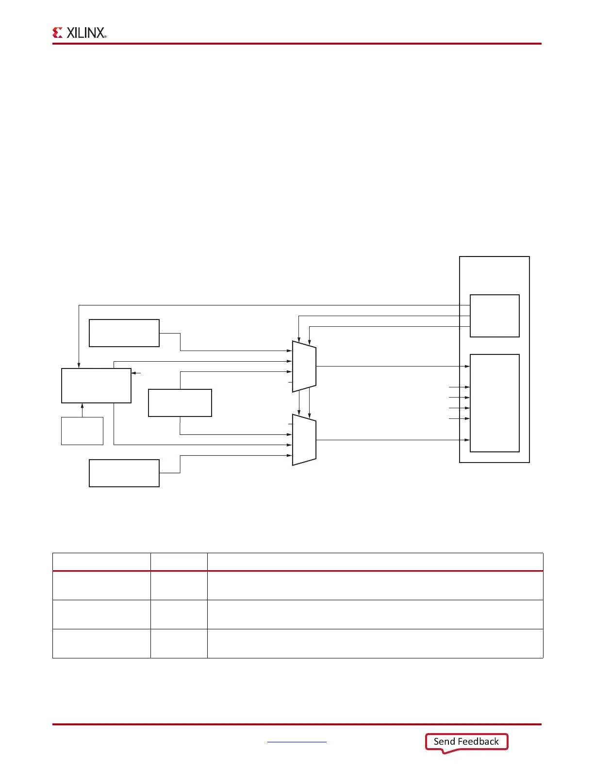
GTP Transceiver Clock Multiplexer
[Figure 1-2, callout 35]
The AC701 board provides flexible GTP Quad 213 MGTREFCLK options through the use
of external multiplexer (MUX) components U3 and U4 to service the GTP Quad 213 SFP,
FMC, and SMA MGT interfaces.
FPGA U1 MGT Bank 213 has two clock inputs, MGTREFCLK0 and MGTREFCLK1. Each
clock input is driven by a series capacitor coupled clock sourced from a SY89544UMG
4-to-1 multiplexer.
Each multiplexer has a clock source at three of its four inputs; the fourth input is not
connected.
The diagram for the GTP Quad 213 clock multiplexer circuit is shown in Figure 1-14.
Table 1-9 lists the MGT sources for U3 and U4. See Table 1-10 and Table 1-11 for details.
X-Ref Target - Figure 1-14
Figure 1-14: AC701 Board GTP 213 U3 and U4 MUX Inputs
UG952_c1_114_012115
Si5324
Jitter Attenuator
CLK Multiplier
U24
GTP SMA
J25(P)/J26(N)
FMC Connector
(HPC)
J30
ICS844021
125 Mhz Clock
U2
X6
Crystal
Oscillator
114.285 MHz
3
2
1
0
U3
0
1
2
3
U4
Rec_Clock_C_P/N Pins D23,D24
SEP_MGT_CLK_SEL[1:0] Pins C24:B26
PCIE_MGT_CLK_SEL[1:0] Pins C26:A24
EPHYCLK_Q0_C_P/N Pins 7,6
SI5324_Out0_C_N/P Pins 29,28
Pins D4,D5
Pins B20,B21
SI5324_Out1_C_P/N Pins 35,34
SMA_MGT_REFCLK_P Pin 1,1
SFP_MGT_CLK0_N/P Pins AA13,AB13
SFP_MGT_CLK1_N/P Pins AA13,AB13
NC
NC
I2C or SPI
FMC DP1
SMA MGT TX/RX
FMC DPO
SFP TX/RX
U1
Artix-7 FPGA
XC7A200T-
2FBG676C
GTP Quad
213
Bank 16
Table 1-9: MGT Clock Multiplexer U3 and U4 Clock Sources
Clock Name Reference Description
125 MHz clock
generator
U2
ICS844021 Crystal-to-LVDS Clock Generator (ICS). See U3 IN0: 125 MHz Clock
Generator, page 32.
Jitter attenuated clock U24
Si5324C LVDS precision clock multiplier/jitter attenuator (Silicon Labs). See U3/
U4 IN1: Jitter Attenuated Clock, page 33.
FMC HPC GBT CLK0
and CLK1
J30
FMC_HPC_GBTCLK0_M2C_C_P/N at U3; FMC_HPC_GBTCLK1_M2C_C_P/
N at U4; See
U3/U4 IN2: FMC HPC GBT Clocks, page 34.

 Loading...


