Chapter
3
31
Data Table
This chapter introduces concepts and terminology necessary for a general
understanding of programmable controller memory. It explains the
memory organization of the PLC-2/30 programmable controller.
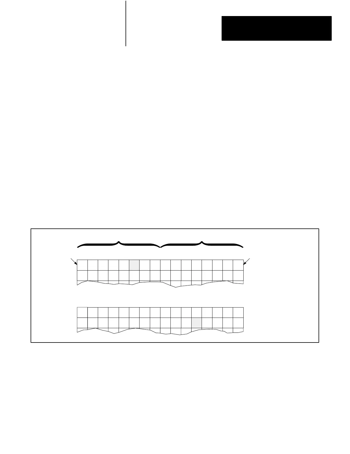
The memory of the processor can be thought of as a large arrangement of
storage points, each called a BInary digiT, or bit (Figure 3.1). A bit is the
smallest unit of information a memory is capable of retaining. Information
stored in each bit is represented as a 1 or 0. When a bit is on, it is
represented by a logic 1. When a bit is off, it is represented by a logic 0.
Figure 3.1
Memory
W
ord Structure
1
0
0
1
1
1
0
1
1
1
0
0
0
1
1
0
0
0
1
0
0
1
0
1
1
0
1
1
1
0
0
1
17 16 15 14 13 12 11 10 07 06 05 04 03 02 01 00
1
0
0
1
0
1
0
1
1
0
0
0
1
0
0
0
0
1
1
1
1
0
0
0
1
0
0
1
0
0
0
0
17 16 15 14 13 12 11 10 07 06 05 04 03 02 01 00
MSB LSB
Upper Byte Lower Byte
Word
Address 030
8
W
ord Address 031
8
W
ord Address 1700
8
W
ord Address 1701
8
Each bit in a word is identified by a two-digit number using the octal
numbering system. Memory bits are numbered 00 through 07 and 10
through 17, with the least significant bit (LSB = 00
8
) at the right and the
most significant bit (MSB = 17
8
) at the left.
A group of 8 bits forms a single byte. A byte is defined as the smallest
complete unit of information that can be transmitted to or from the
processor at a given time.
3.0
General
3.1
Memory Structure
Artisan Technology Group - Quality Instrumentation ... Guaranteed | (888) 88-SOURCE | www.artisantg.com
 Loading...