11-4 403 – 447 MHz UHF1 Theory Of Operation: UHF1 Frequency Generation Circuitry
11.3.4 Auto Power Control
The APC keeps the current supply constant to the final amp (Q403). The drain current of Q403 (final
amp) is sensed across resistor R417. The differential signal at the output of U401 (Pin 7) is passed to
Q404 and Q405 that produces a constant power output to the antenna. If the current is changed due
to change of battery voltage or load, APC controls gate voltage of Q403 and collector voltage of Q401
and drain voltage of Q402 to keep TX power stable. This circuit stabilizes TX power at a pre-
determined level adjusted by U402. This bias voltage is tuned in the factory. If the transistor (Q403) is
replaced, the RF Output Power must be tuned. By tuning the RF output power, the bias voltage will be
tuned through U402. Extra care has to be taken during the tuning process. Do not exceed the
maximum allowed bias voltage.
11.4 UHF1 Frequency Generation Circuitry
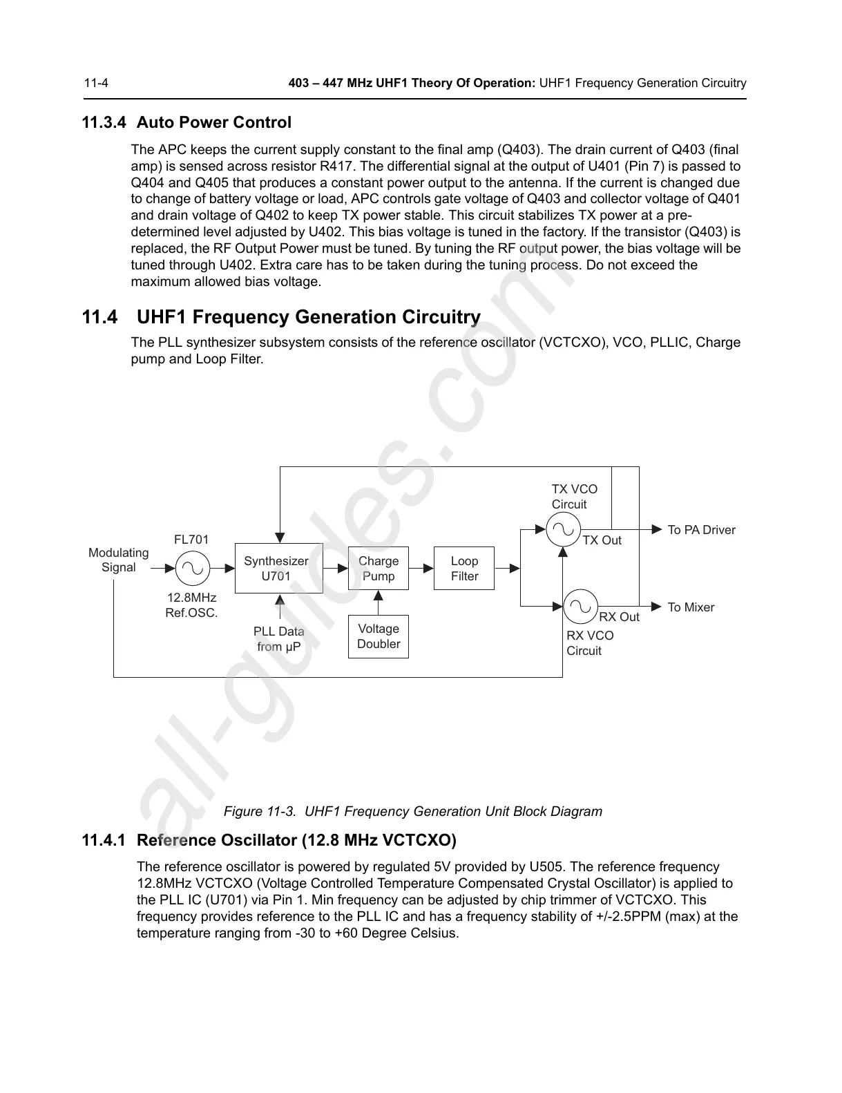
The PLL synthesizer subsystem consists of the reference oscillator (VCTCXO), VCO, PLLIC, Charge
pump and Loop Filter.
Figure 11-3. UHF1 Frequency Generation Unit Block Diagram
11.4.1 Reference Oscillator (12.8 MHz VCTCXO)
The reference oscillator is powered by regulated 5V provided by U505. The reference frequency
12.8MHz VCTCXO (Voltage Controlled Temperature Compensated Crystal Oscillator) is applied to
the PLL IC (U701) via Pin 1. Min frequency can be adjusted by chip trimmer of VCTCXO. This
frequency provides reference to the PLL IC and has a frequency stability of +/-2.5PPM (max) at the
temperature ranging from -30 to +60 Degree Celsius.
Modulating
Signal
FL701
12.8MHz
Ref.OSC.
Charge
Pump
Loop
Filter
TX VCO
RX Out
To Mixer
To PA Driver
TX Out
Circuit
RX VCO
Circuit
Voltage
Doubler
Synthesizer
U701
PLL Data
from μP
 Loading...