435 – 480 MHz UHF2 Theory of Operation: UHF2 Frequency Generation Circuitry 5-5
5.4 UHF2 Frequency Generation Circuitry
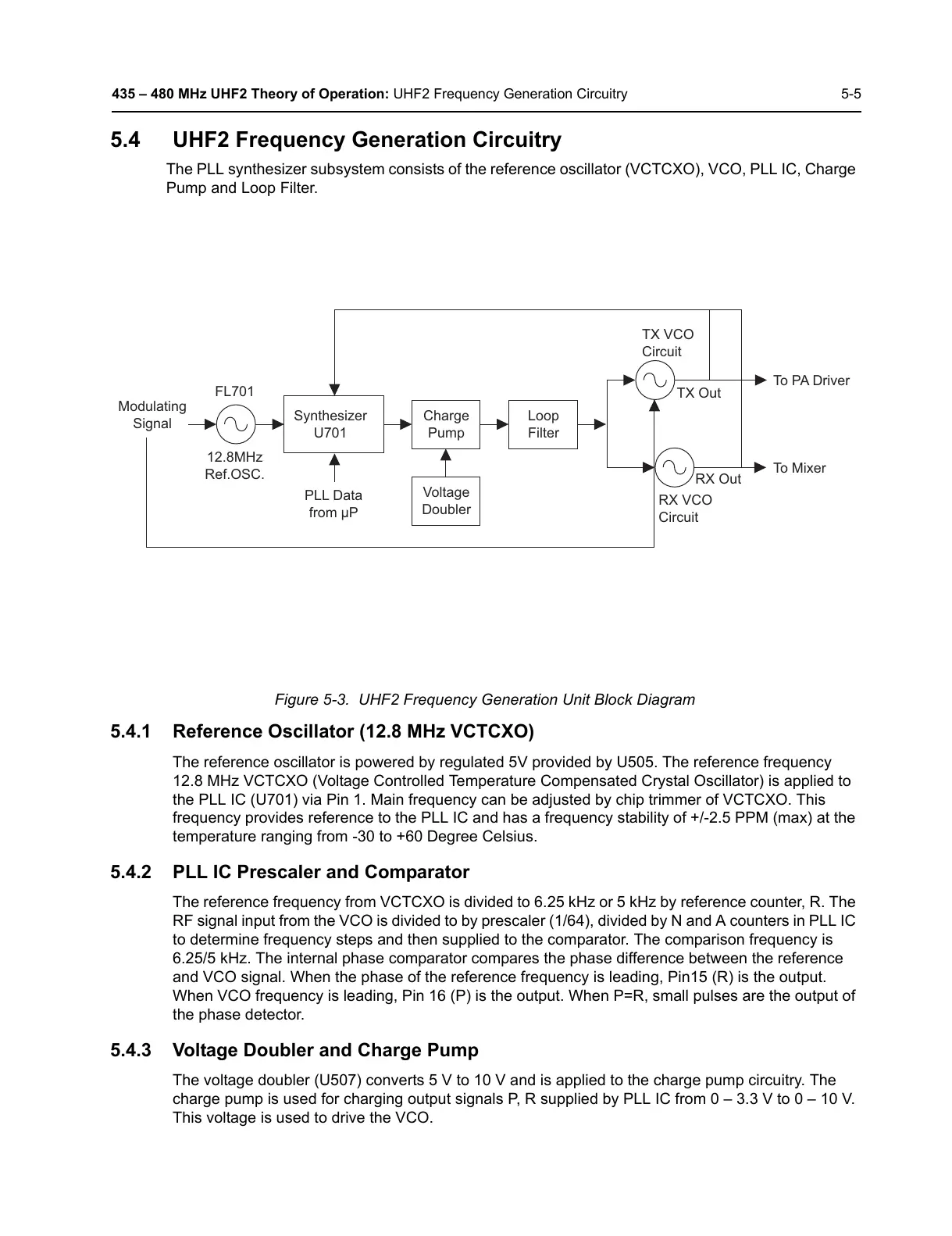
The PLL synthesizer subsystem consists of the reference oscillator (VCTCXO), VCO, PLL IC, Charge
Pump and Loop Filter.
Figure 5-3. UHF2 Frequency Generation Unit Block Diagram
5.4.1 Reference Oscillator (12.8 MHz VCTCXO)
The reference oscillator is powered by regulated 5V provided by U505. The reference frequency
12.8 MHz VCTCXO (Voltage Controlled Temperature Compensated Crystal Oscillator) is applied to
the PLL IC (U701) via Pin 1. Main frequency can be adjusted by chip trimmer of VCTCXO. This
frequency provides reference to the PLL IC and has a frequency stability of +/-2.5 PPM (max) at the
temperature ranging from -30 to +60 Degree Celsius.
5.4.2 PLL IC Prescaler and Comparator
The reference frequency from VCTCXO is divided to 6.25 kHz or 5 kHz by reference counter, R. The
RF signal input from the VCO is divided to by prescaler (1/64), divided by N and A counters in PLL IC
to determine frequency steps and then supplied to the comparator. The comparison frequency is
6.25/5 kHz. The internal phase comparator compares the phase difference between the reference
and VCO signal. When the phase of the reference frequency is leading, Pin15 (R) is the output.
When VCO frequency is leading, Pin 16 (P) is the output. When P=R, small pulses are the output of
the phase detector.
5.4.3 Voltage Doubler and Charge Pump
The voltage doubler (U507) converts 5 V to 10 V and is applied to the charge pump circuitry. The
charge pump is used for charging output signals P, R supplied by PLL IC from 0 – 3.3 V to 0 – 10 V.
This voltage is used to drive the VCO.
Modulating
Signal
FL701
12.8MHz
Ref.OSC.
Charge
Pump
Loop
Filter
TX VCO
RX Out
To Mixer
To PA Driver
TX Out
Circuit
RX VCO
Circuit
Voltage
Doubler
Synthesizer
U701
PLL Data
from μP
 Loading...