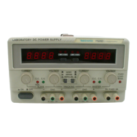
Theory of Operation-PS
SO
1
0
Internally, all four DACs employ a current reference driv-
ing a ladder network. Each bit drives a binary weighted cur-
rent switch that steers the current into either lout or
m.
The negative current sources (pins 2 and 4) in U1221 and
U1230 are transistor collectors. This gives the lout terminal
a voltage compliance of
-
10 V to
+
18 V. The current
sources in voltage DACs U1130 and U1231 are taps on the
passive ladder network thus requiring termination of lout
and into exactly the same voltage as the ladder ground
(pin 3). The reference for the current DACs U1221 and
U 1230 is provided by VR 1 1 1 1. The reference current is de-
termined the same as in the logic supply DACs, as previous-
ly described. However, in the floating supply, voltage divider
R1100 and R1101 program the logic threshold of U1221
and U1230 to match the shift register output.
The entire voltage DAC reference circuit tracks the com-
mon sensing input (ground 2). A +6.2 V reference is gener-
ated by temperature compensated Zener VR1340. The
Zener diode is driven by constant current source
(21340,
R1347, R1346, and VR1341. R1530 sinks about the same
current from ground 2 (common sensing input) to
-
15 V,
minimizing the loading on the common sensing line. The cur-
rent source is off when the reference disable line is high.
When the current source is off,
R1349 pulls the reference
voltage negative. Diode
CR1340 then clamps this level at
about
-
700
mV.
The reference is disabled during the out-
put off sequence.
The reference voltage is buffered by U1330C and invert-
ed by U1330D. The resulting
+
and -6.2 V drive the refer-
ence inputs of voltage DACs U1130 and U1231. Both
voltages also drive a divider network with four zero adjust-
ments. R1335 and R1334 null out the offset voltage in the
+V
and -V current to voltage converters, U1330B and
U1330A respectively. To meet differential linearity specifica-
tion (step size accuracy), this voltage must be nulled to
~200 pV. R1345 and R1344 are zero adjustments for the
i
and
-
output voltage.
R1340 and R1327, along with C1231 and C1230, are
compensation networks for the current to voltage convert-
ers. Schottky diodes CR1130 and CR1220 protect the lout
outputs from negative excursions on power up. The current
to voltage converter feedback to resistor is connected to pin
16 inside the DAC.
The output of the
-
current DAC is converted to voltage
via U1111 A. The zero adjust for this converter is R1321 in
conjunction with the associated resistive dividers. These
dividers operate between
+
15 V and
-
15 V. Current to
voltage conversions for the
+
current DAC is provided by
R1211 and R1210. The 0 adjust for this converter is pro-
vided
by
R1311. This signal is buffered by unity gain follow-
er U1111B.
+
Floating
Supply
The output of the
+
current DAC connects to pin 3 of
U1100. The
+
current sense from sensing resistor R1104
connects to pin 2 of U1100. As the supply output current
increases, the voltage at pin 2 of U1100 goes more negative
with respect to the output common (ground 1). When the
current sense voltage equals the current
DAC voltage, the
output, pin
6,
of U1100 goes positive. This signal, along with
the
-
voltage error amplifier output, increases conduction in
Q14O2. This lowers the base voltage on (21401, Q1400, and
the two series pass-transistors in the power module, result-
ing in a lower output voltage.
To set the output voltage, the +V sense is combined
through a resistive divider consisting of R1533, R1545,
R1543, R1542, R1544, and R1541 with the negative volt-
age from the +V DAC. If the 10 V range is selected, (21640
is on and (21641 is off. If the 32 V range is selected, (21641
conducts, selecting the 32 V divider to be applied to pin 3 of
U1420. The voltage at pin 2 of U1420 comes from R1345
and has a range of 220 mV from the common sensing
point. When a change in output load lowers the output volt-
age, the sense line voltage lowers the common input of
dividers
R
1 533 and R 1 541
.
This lowers pin 3 of U 1420,
which reduces conduction in (21402. This action raises the
base voltage of Q1401, which tracks through the Darlington
triple output stage increasing the output voltage. CR1420
and VR1420 prevent saturation and slow recovery of U 1420
in under and over-voltage conditions. The
+
sense line is
connected to the
+
output terminal through CR1500 and
CR1510. These diodes prevent the sense line from moving
more than one diode drop from the
+
output bus. The
emitter of Q1400 is connected to pin 3 of U1420 through
C1410. This capacitor provides high frequency compensa-
tion for the amplifier.
A
10
!IF
capacitor, C1531, is connected from the
+
out-
put terminal to common. A current sink contributes stability
and provides a rapid discharge path for
C1531.
S1500 selects the front panel or the rear interface out-
puts and sense lines. The unused ports are floating.
The emitters of the series pass-transistors are balanced
through
R1622, R1611, and R1612. When the power supply
is operated in the standard compartment of a power mod-
ule, the high power switch S1600A is open. The emitter re-
sistor for the high power series pass-transistor is 0.75
!1
(R1611). In the high power compartment, St 600A is closed,
shunting R16ll with R1612. This increases the current
through the high power transistor to approximately two
times that passing through the standard transistor.
 Loading...