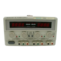
Section 4-PS 50 10
THEORY
OF
OPERATION
LOGIC AND FLOATING
SUPPLY
BLOCK DIAGRAM DESCRIPTION
Introduction
If the voltage across the sense resistor exceeds the cur-
rent DAC voltage, the output of the error amplifier takes
The
PS
501
has
three
regulated
Output
and
several
in-
control of the series pass-transistor and limits the output
ternal
su~~lies'
The
Output
su~~lies
are
the
su~~l~y
current to the value
of
the programmed current.
and the POSITIVE and NEGATIVE floating supplies.
Logic
Supply
Block Diagram
Referring to the first block diagram in the pullout pages
at the rear of this manual, +26 V, -26 V, and
+8
V from
the mainframe are filtered in the input filter and control sup-
ply block. This supply provides all voltage is needed to oper-
ate the CPU and the control voltages for the logic supply.
The logic supply consists of an internally mounted
pass-
transistor whose collector is connected to the
+8
V
and the
necessary control circuitry. The regulation and control cir-
cuitry is divided into three sections. The outputs of these
three sections are
ORd together at the base of the series
pass-transistor. These circuits are the current loop, voltage
loop, and the fold-back current limit circuit.
Remote voltage sensing is provided for the common and
the output terminals. The output of the logic supply ranges
from 4.5
V
to 5.5 V. The reference voltage is generated from
a 4.5
V
signal that track.s the common or ground sense. This
4.5
V
signal is summed with the output of a
0
to
1
V digital-
to-analog converter driven by the CPU, resulting in a 4.5 V
to
5.5
V
signal referenced to the ground sense. This signal
passes to the voltage error amplifier and is compared with
the output voltage from the remote sense line.
The current sense resistor is in series with the
pass-tran-
sistor and the output terminal. The voltage drop across this
resistor is proportional to the logic supply current.
The output voltage of the logic current DAC is propor-
tional to the programmed current limit.
The fold-back current limit checks the output voltage and
current. This circuit protects the pass-transistor from
overdissipation when the supply is operated outside of the
specified load range. This is done by lowering the current
limit point until transistor dissipation is within a safe region.
The outputs of the current and voltage loops are monitored
by the loop balance status comparators. These compara-
tors serve as inputs to the CPU. In normal operation one of
the loops
IS
balanced. In the fold-back condition or
overvoltage condition neither loop is balanced.
Floating
Supply
Block Diagram
As shown on block diagram
2,
floating supply power is
derived from the isolated ac windings in the mainframe. The
rectifier, filter, and control supply are two power supplies
whose commons are not directly connected. The
+
and
-
commons are connected through the sense resistors to
form the common for both floating supplies. This is the
front-panel common return.
The
-+
15 V control supplies are referenced to the front-
panel common terminal. These control supplies are used
throughout the floating supply control circuitry.
The
+
collector supply voltages for the series pasqtran-
sistors are filtered but unregulated. The base drive for the
series pass-transistors is regulated at either +24
V
or
+40
V
depending on the position of the mode relay. If the
power supply is programmed for a current greater than
750
mA, (400 mA in a standard compartment) the collector
switches to the
+
24
V
supply. The collector voltage
changes range with the base drive to prevent
overdissipation of the pass-transistors.
The
DAC
voltage is compared to the sense resistor volt-
As the
$-
and
-
floating supplies are identical, except for
age
by
the current error amplifier.
polarities, only the
+
supply is described. The voltage at the
 Loading...