~-------
~
945424-9701
CHASSIS
SELECT
CRU
ADDRESS
FORMAT
MODULE
SELECT
BIT
SELECT
Figure 1-6. CRU 12-Bit Addressing Scheme
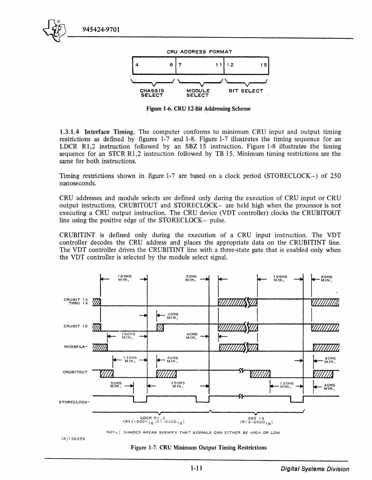
1.3.1.4 Interface Timing. The
computer
conforms
to
mimmum CRU
input
and
output
timing
restrictions as defined by ·figures
1-
7 and 1-8. Figure
1-
7 illustrates the timing sequence for an
LDCR
Rl,2
instruction followed
by
an
SBZ
15
instruction. Figure 1-8 illustrates
the
timing
sequence for an STCR
Rl
,2 instruction followed
by
TB
15. Minimum timing restrictions are
the
same for
both
instructions.
Timing restrictions shown in figure
1-7
are based
on
a clock period
(STORECLOCK-)
of
250
nanoseconds.
CRU addresses and module selects are defined only during the execution
of
CRU
input
or
CRU
output
instructions. CRUBITOUT and
STORECLOCK-
are held high when the processor is
not
executing a CRU
output
instruction. The CRU device (VDT controller) clocks the CRUBITOUT
line using the positive edge
of
the
STORECLOCK-
pulse.
CRUBITINT
is
defined only during
the
execution
of
a CRU
input
instruction. The VDT
controller decodes the CRU address and places the appropriate
data
on
the CRUBITINT line.
The VDT controller drives the CRUBITINT line with a three-state gate
that
is
enabled only when
the VDT controller is selected
by
the module select signal.
CRUBIT
1 2
THRU
14
CRUBIT
1 5
MODSELA-
CRUBITOUT
STORECLOCK-
(A)
1
36255
I
WJ
185NS
MIN.
1.-
160NS
1
_
MIN.
!.--
135NS
I
MIN.
SONS
1
MIN,
LJ
I.--
40NS
1
_
MIN.
250NS
MIN,
LDCR
R 1 , 2
(Rl2=0000
16
,~1~o~00
16
)
35NS
MIN.
40NS
MIN,
LJ
SS
SBZ
15
185NS
MIN.
L135NS
r
-MIN,
LJ
(R
12=0000
1
6
)
NOl
C.:
SHADED
AREAS
SIGNIFY
THAT
SIGNALS
CAN
E!THER
BE
HIGH
OR
LOW
Figure
1-7.
CRU Minimum Output Timing Restrictions
14--
85NS
I
MIN.
L40NS
,-
MIN.
L
40NS
!MIN,
1-11
Digital Systems Division
 Loading...