~~-~--------~~~-
~
945424-9701
Keyboard Parity Error (CR U
Input
Bit
E
16
).
When Keyboard Parity Error = 1,
it
indicates
that
a
parity
error
existed during
the
last keyboard
data
transmission. Keyboard Parity
Error
is
valid
only
if
Keyboard Data Ready (CRU
Input
Bit F
16
) =
1.
Keyboard Acknowledge (CRU
output
bit
D
16
with CRU
output
bit
F
16
= 1) resets Keyboard Parity Error.
Keyboard Data
Ready
(CR U
Input
Bit
F
16
) . Keyboard Data Ready is set
to
1
by
the
VDT
controller when Keyboard Data
is
ready
to
be addressed and read
by
the
computer. Keyboard
Data Ready is reset
by
Keyboard Acknowledge.
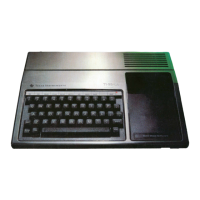
1.3.2 KEYBOARD-TO-POWER/LOGIC
PWB
INTERFACE. The interface between
the
keyboard
and
the
power/logic pwb in
the
display
unit
cabinet
is
implemented
by
an
interconnection
cable
that
connects directly
to
the power /logic pwb inside
the
display
unit
cabinet. Figure 1-11
illustrates
the
interface, and
the
following paragraphs describe
the
signals
on
the
interface.
1.3.2.1 Keyboard Data (KBDT,1-8). Keyboard Data are
the
high-active eight-bit codes produced
by
the
keyboard encoder for each
data
key
on
the
keyboard.
1.3.2.2
Keyboard
Data Strobe
(KBSIN-).
Keyboard Data Strobe
is
the
low-active
20-microsecond (nominal) strobe signal produced
by
the
keyboard
encoder
each time
new
data
is
stable
on
the
Keyboard Data lines.
1.3.2.3 Repeat
(REPEAT-).
Repeat is the low-active
output
of
the
REPEAT key, and
is
used
to
drive
the
repeat logic
on
the
power/logic pwb
to
cause repetition
of
the
code carried
by
Keyboard Data
at
10 ±2 hertz whenever Repeat is active prior
to
Keyboard Data Strobe.
1.3.3 POWER/LOGIC PWB-TO-VDT CONTROLLER INTERFACE. The interface
between
the
power/logic pwb and the VDT controller
is
implemented
by
an interconnection cable.
Figure 1-12 illustrates
the
interface signals originated by
the
power/logic pwb for
the
VDT
controller. The signals produced
by
the
VDT controller for
the
power/logic pwb also travel
on
the
same interconnection cable, and are discussed
;n
a
later
paragraph. The following paragraphs
describe
the
signals from the power/logic pwb
to
the VDT controller.
1.3.3.1 Keyboard Data (TET,1,2,T).
Keyboa~u
Data are complementary
outputs
of
a differential
line driver
on
the
power/logic pwb. These signals travel
on
a pair
of
lines
that
carry
the
serial
11-bit keyboard code with start,
stop
and parity bits
to
the
VDT controller. The format for
the
11-bit code is shown in figure 1-13.
1.3.3.2 Terminal Ready (TRD,1,2,T). The Terminal Ready signals are complementary
outputs
of
a differential line driver on the power/logic pwb. These
two
signals provide the indication
of
whether
the
terminal
is
operational
to
the
computer
via
the
VDT controller.
If
TRD 1 T = 0 and
TRD2T
=
1,
the
condition
is
an indication
of
loss
of
horizontal synchronization signals from
the
VDT controller
or
loss
of
power from
the
power supply.
1.3.4 VDT CONTROLLER-TO-POWER/LOGIC
PWB
INTERFACE. The interface between
the
VDT controller
and
the power/logic pwb in the display
unit
cabinet is implemented
by
the
same
interconnection cable and wiring harness described in paragraph 1.3.3. Figure 1-14 illustrates
the
interface signals produced
by
the
VDT controller for
the
power/logic pwb.
1-19
Digital
Systems Division
 Loading...