1
SBAU171D–May 2010–Revised January 2016
Submit Documentation Feedback
Copyright © 2010–2016, Texas Instruments Incorporated
ADS1298ECG-FE/ADS1198ECG-FE
User's Guide
SBAU171D–May 2010–Revised January 2016
ADS1298ECG-FE/ADS1198ECG-FE
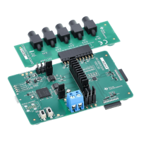
This user's guide describes the characteristics, operation, and use of the ADS1298ECG-FE and
ADS1198ECG-FE. The ADS1298ECG-FE and ADS1198ECG-FE are evaluation modules for the
ADS1298, an eight-channel, 24-bit, and ADS1198, an eight-channel, 16-bit, analog-to digital converter
(ADC). Both devices provide low-power, integrated analog front-end (AFE) designs for patient monitoring
and portable and high-end electrocardiogram (ECG) and electroencephalogram (EEG) applications. This
user's guide includes a complete circuit description, schematic diagram, and bill of materials.
The following related documents are available through the Texas Instruments web site at www.ti.com.
Device Literature Number
ADS1298 SBAS459
ADS1198 SBAS471
Contents
1 ADS1298ECG-FE/ADS1198ECG-FE Overview......................................................................... 3
1.1 Important Disclaimer Information ................................................................................. 3
1.2 Introduction .......................................................................................................... 4
1.3 Supported Features ................................................................................................ 4
1.4 Features Not Supported in Current Version..................................................................... 4
1.5 ADS1x98ECG-FE Hardware ...................................................................................... 5
1.6 Minimum System Requirements for ADS1x98ECG-FE Evaluation Software............................... 5
2 Quick Start.................................................................................................................... 6
2.1 Default Jumper/Switch Configuration ............................................................................ 6
2.2 ADS1x98ECG-FE Operation...................................................................................... 7
3 Using the ADS1298ECG-FE Software.................................................................................... 8
3.1 Application User Menu ............................................................................................. 9
3.2 Top-Level Application Controls ................................................................................... 9
3.3 About Tab .......................................................................................................... 10
3.4 ADC Register Tab................................................................................................. 11
3.5 Analysis Tab ....................................................................................................... 19
3.6 Save Tab ........................................................................................................... 27
4 ADS1x98ECG-FE Input Signals.......................................................................................... 29
4.1 Input Short Testing................................................................................................ 29
4.2 Internal Test Signals Input ...................................................................................... 29
4.3 Temperature Sensor.............................................................................................. 30
4.4 Normal Electrode Input .......................................................................................... 31
4.5 MV
DD
Input, RLD Measurement, RLD Positive Electrode Driver, and RLD Negative Electrode Driver 31
4.6 Lead Derivation.................................................................................................... 32
4.7 Wilson Center Terminal (WCT).................................................................................. 32
4.8 Right Leg Drive .................................................................................................... 32
4.9 PACE Detection ................................................................................................... 33
5 ADS1298ECG-FE/ADS1198ECG-FE Hardware Details .............................................................. 35
5.1 Jumper Description ............................................................................................... 36
5.2 Power Supply ...................................................................................................... 37
5.3 Clock ................................................................................................................ 38
5.4 Reference .......................................................................................................... 38
5.5 Analog Output Signals............................................................................................ 39